 | ÐлекÑÑоннÑй компоненÑ: GMS82512 | СкаÑаÑÑ:  PDF PDF  ZIP ZIP |
Äîêóìåíòàöèÿ è îïèñàíèÿ www.docs.chipfind.ru

HYUNDAI MICRO ELECTRONICS
8-BIT SINGLE-CHIP MICROCONTROLLERS
GMS82512
GMS82516
GMS82524
MicroElectronics
Semiconductor Group of Hyundai Electronics Industrial Co., Ltd.
User's Manual (Ver. 1.00)

Version 1.00
Published by
MCU Application Team
©
©
©
©
2000 HYUNDAI MicroElectronics All right reserved.
Additional information of this manual may be served by HYUNDAI MicroElectronics offices in Korea or Distributors and
Representatives listed at address directory.
HYUNDAI MicroElectronics reserves the right to make changes to any information here in at any time without notice.
The information, diagrams and other data in this manual are correct and reliable; however, HYUNDAI Micro Electronics is
in no way responsible for any violations of patents or other rights of the third party generated by the use of this manual.

HYUNDAI MicroElectronics
GMS82512/16/24
FEB. 2000 Ver 1.00
1
Table of Contents
1. OVERVIEW ...........................................1
Description .........................................................1
Features .............................................................1
Development Tools ............................................2
Ordering Information ..........................................2
2. BLOCK DIAGRAM ................................3
3. PIN ASSIGNMENT ...............................4
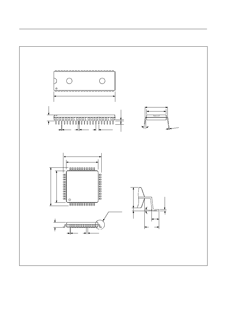
4. PACKAGE DIAGRAM
.............................. 5
5. PIN FUNCTION .....................................6
6. PORT STRUCTURES ...........................8
7. ELECTRICAL CHARACTERISTICS ...10
Absolute Maximum Ratings .............................10
Recommended Operating Conditions ..............10
A/D Converter Characteristics .........................10
DC Electrical Characteristics ...........................11
AC Characteristics ...........................................12
Typical Characteristic Curves ..........................13
8. MEMORY ORGANIZATION ................15
Registers ..........................................................15
Program Memory .............................................18
Data Memory ...................................................21
Addressing Mode .............................................24
9. I/O PORTS ..........................................28
10. BASIC INTERVAL TIMER .................31
11. TIMER/EVENT COUNTER ...............33
8-bit Timer / Counter Mode ..............................35
16-bit Timer / Counter Mode ............................39
8-bit Capture Mode ..........................................40
16-bit Capture Mode ........................................41
12. ANALOG DIGITAL CONVERTER ....43
13. BUZZER FUNCTION ........................45
14. INTERRUPTS ...................................47
Interrupt Sequence .......................................... 49
BRK Interrupt .................................................. 50
Multi Interrupt .................................................. 51
External Interrupt ............................................. 51
15. WATCHDOG TIMER ........................54
16. POWER DOWN OPERATION ..........56
STOP Mode .................................................... 56
Minimizing Current Consumption .................... 57
17. OSCILLATOR CIRCUIT ....................59
18. RESET ..............................................60
External Reset Input ........................................ 60
Watchdog Timer Reset ................................... 60
19. POWER FAIL PROCESSOR ............61
20. OTP PROGRAMMING ......................63
How to Program .............................................. 63
Pin Function .................................................... 63
Programming Specification ............................. 65
A. CONTROL REGISTER LIST ................. i
B. SOFTWARE EXAMPLE ....................... ii
7-segment LED display .....................................ii
C. INSTRUCTION ................................... vii
Terminology List ............................................... vii
Instruction Map ................................................ viii
Alphabetic order table of instruction ..................ix
Instruction Table by Function .......................... xiv
D. MASK ORDER SHEET
......................... xx
HYUNDAI MicroElectronics
GMS82512/16/24
FEB. 2000 Ver 1.00
1
GMS82512/16/24
CMOS SINGLE-CHIP 8-BIT MICROCONTROLLER
WITH A/D CONVERTER
1. OVERVIEW
1.1 Description
The GMS82512/16/24 are advanced CMOS 8-bit microcontrollers with 12K/16K/24K bytes of ROM. The device is one of
GMS800 family. This device using the GMS800 family CPU includes several peripheral functions such as Timer, A/D con-
verter, Programmable buzzer driver, etc. The RAM, ROM, and I/O are placed on the same memory map in addition to simple
instruction set.
1.2 Features
· 12K/16K/24K Bytes On-chip Program Memory
· 448 Bytes of On-chip Data RAM
(Included stack memory)
· Minimum Instruction Execution Time
0.5
µ
µ
µ
µ
s at 8MHz
· One 8-bit Basic Interval Timer
· Four 8-bit Timer/Event counter
or Two 16-bit Timer/Event counter
· One 6-bit Watchdog timer
· Four channel 8-bit A/D converter
· Four External Interrupt input ports
· Buzzer Driving port
- 500Hz ~ 250kHz@8MHz
· 35 I/O Ports
· Eleven Interrupt sources
- Basic Interval Timer: 1
- External input: 4
- Timer/Event counter: 4
- ADC: 1
- WDT: 1
· Built in Noise Immunity Circuit
- Noise filter
- Power fail processor
· Power Down Mode
- STOP mode
· 2.2V to 5.5V Wide Operating Range
· 1~10MHz Wide Operating Frequency
· 42SDIP, 44QFP package types
· Available 24K bytes OTP version
Device name
ROM Size
RAM Size
OTP
Package
GMS82512
12K bytes
448 bytes
GMS82524T
42SDIP, 44QFP
GMS82516
16K bytes
448 bytes
GMS82524T
GMS82524
24K bytes
448 bytes
GMS82524T
GMS82512/16/24
HYUNDAI MicroElectronics
2
FEB. 2000 Ver 1.00
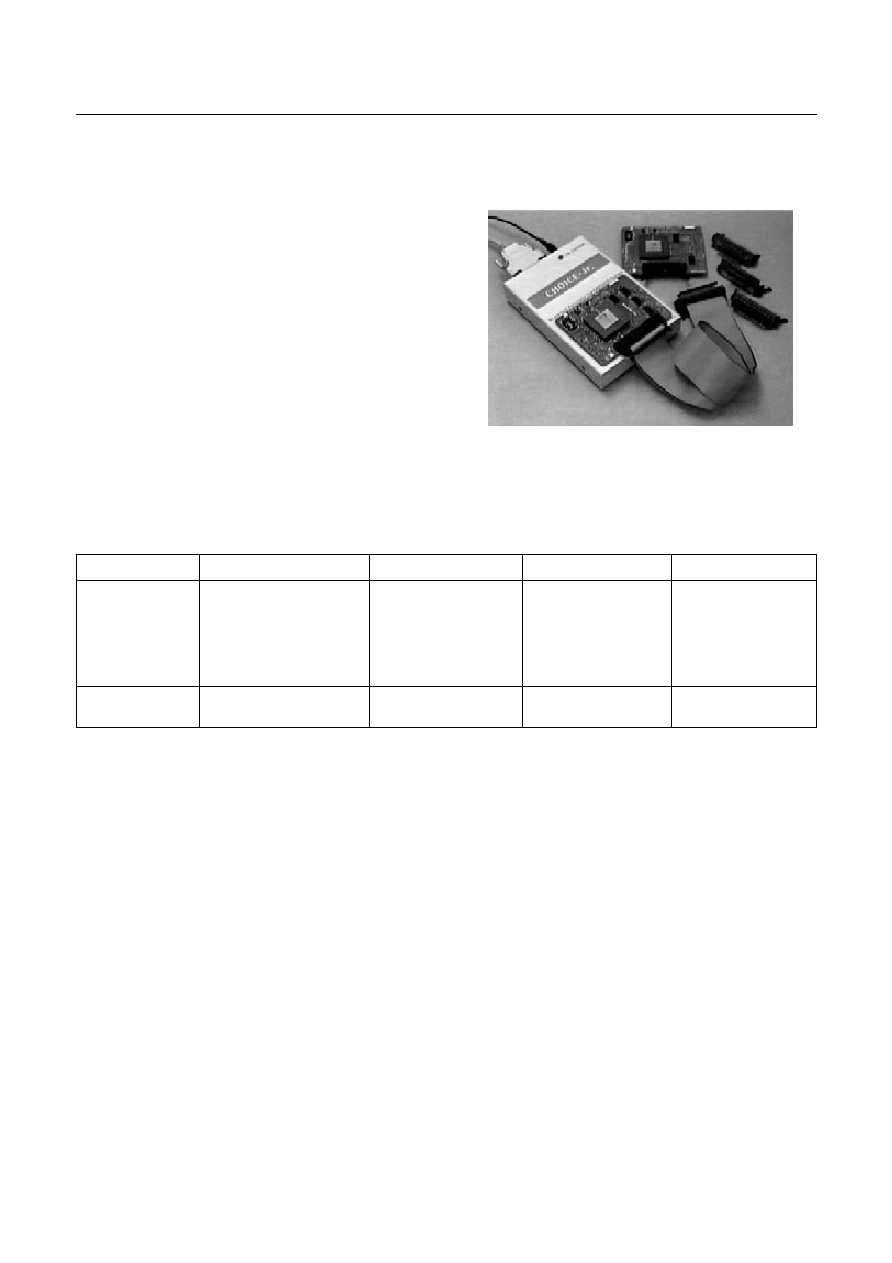
1.3 Development Tools
The GMS825xx is supported by a full-featured macro as-
sembler, an in-circuit emulator CHOICE-Jr.
TM
and OTP
programmers. There are third different type programmers
such as emulator add-on board type, single type, gang type.
For mode detail, Refer to "20. OTP PROGRAMMING" on
page 63. Macro assembler operates under the MS-Win-
dows 95/98
TM
.
Please contact sales part of HYUNDAI MicroElectronics.
1.4 Ordering Information
Device name
ROM Size
RAM size
Package
Mask version
GMS82512 K
GMS82512 Q
GMS82516 K
GMS82516 Q
GMS82524 K
GMS82524 Q
12K bytes
12K bytes
16K bytes
16K bytes
24K bytes
24K bytes
448 bytes
448 bytes
448 bytes
448 bytes
448 bytes
448 bytes
42SDIP
44QFP
42SDIP
44QFP
42SDIP
44QFP
OTP version
GMS82524T K
GMS82524T Q
24K bytes OTP
24K bytes OTP
448 bytes
448 bytes
42SDIP
44QFP
HYUNDAI MicroElectronics
GMS82512/16/24
FEB. 2000 Ver 1.00
3
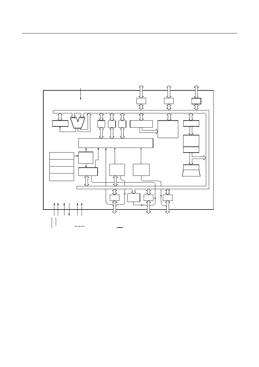
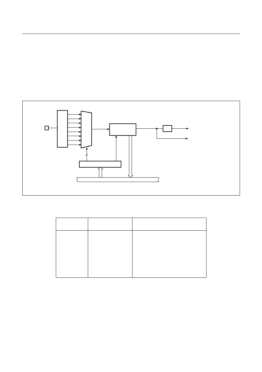
2. BLOCK DIAGRAM
ALU
A
Interrupt Controller
Data Memory
8-bit
ADC
8-bit
Counter
Timer/
Program
Memory
Data Table
PC
8-bit Basic
Timer
Interval
Watchdog
Timer
PC
R4
R5
R0
PSW
System controller
Timing generator
System
Clock Controller
ClockGenerator
RES
E
T
TE
ST
X
IN
X
OU
T
R40 / INT0
R41 / INT1
R42 / INT2
R43 / INT3
R44 / EC0
R00~R07
V
DD
V
SS
Power
Supply
R54 / WDTO
R55 / BUZ
R2
R20~R27
Buzzer
Driver
R6
R64 / AN4
R65 / AN5
R66 / AN6
R67 / AN7
(448 bytes)
AV
DD
ADC Power
Supply
Stack Pointer
X
Y
R3
R30~R37
GMS82512/16/24
HYUNDAI MicroElectronics
4
FEB. 2000 Ver 1.00
3. PIN ASSIGNMENT
R30
V
DD
TEST
AV
DD
R67
R66
R65
R64
R55
R54
R44
R43
R42
R41
R40
RESET
AN7
AN6
AN5
AN4
BUZ
WDTO
EC0
INT3
INT2
INT1
INT0
XIN
XOUT
V
SS
R27
R26
R31
R32
R33
R34
R35
R36
R37
R00
R01
R02
R03
R04
R05
R06
R07
R20
R21
R22
R23
R24
R25
42SDIP
1
2
3
4
5
6
7
8
9
10
11
12
13
14
15
16
17
18
19
20
21
42
41
40
39
38
37
36
35
34
33
32
31
30
29
28
27
26
25
24
23
22
G
M
S
8
2
512/
16/
24
(Top View)
(Top View)
R21
R22
R23
R24
R25
R26
R27
V
SS
XOUT
XIN
RESET
R37
R00
R01
R02
R03
R04
R05
R06
R07
N.
C.
*
R20
R66
R65
R64
N.
C.
*
R55
R54
R44
R43
R42
R41
R40
1
2
3
4
5
6
7
8
9
10
11
R36
R35
R34
R33
R32
R31
R30
V
DD
TEST
AV
DD
R67
33
32
31
30
29
28
27
26
25
24
23
17
16
15
14
13
12
34
35
36
37
38
39
40
41
42
43
44
GMS82512/16/24
44QFP
AN6
AN5
AN4
BUZ
WDT
O
EC0
INT
3
IN
T
2
IN
T
1
IN
T
0
AN7
18
19
20
21
22
N .C .
*
: N o C on nectio n
HYUNDAI MicroElectronics
GMS82512/16/24
FEB. 2000 Ver 1.00
5
4. PACKAGE DIAGRAM
44QFP
2.35 max.
SEE DETAIL "A"
1.03
0.73
0-7
°
0.
2
5
0.
1
0
1.60
Typ.
DETAIL "A"
UNIT: MM
0.45
0.30
0.80 Typ.
2.
10
1.
95
0.
23
0.
13
10.10
9.90
13.45
12.95
10
.
1
0
9.
9
0
13
.
4
5
12.
95
UNIT: INCH
1.465
1.455
0.022
0.016
0.045
0.035
0.070 Typ.
0.
140
0.
120
mi
n.
0.
015
0.545
0.535
0.600 Typ.
0-15
°
42SDIP
0.012
0.008
0
.
19
0 m
a
x.
GMS82512/16/24
HYUNDAI MicroElectronics
6
FEB. 2000 Ver 1.00
5. PIN FUNCTION
V
DD
: Supply voltage.
V
SS
: Circuit ground.
TEST: Used for Test Mode. For normal operation, it
should be connected to V
DD
.
RESET: Reset the MCU.
X
IN
: Input to the inverting oscillator amplifier and input to
the internal main clock operating circuit.
X
OUT
: Output from the inverting oscillator amplifier.
R00~R07: R0 is an 8-bit CMOS bidirectional I/O port. R0
pins 1 or 0 written to the Port Direction Register, can be
used as outputs or inputs.
R20~R27: R2 is an 8-bit CMOS bidirectional I/O port. R2
pins 1 or 0 written to the Port Direction Register can be
used as outputs or inputs.
R30~R37: R3 is an 8-bit CMOS bidirectional I/O port. R3
pins 1 or 0 written to the Port Direction Register can be
used as outputs or inputs.
R40~R44: R4 is an 5-bit CMOS bidirectional I/O port. R4
pins 1 or 0 written to the Port Direction Register can be
used as outputs or inputs.
In addition, R4 serves the functions of the various follow-
ing special features.
R54~R55: R5 is an 2-bit CMOS bidirectional I/O port. R5
pins 1 or 0 written to the Port Direction Register can be
used as outputs or inputs.
In addition, R5 serves the functions of the various follow-
ing special features.
R64~R67: R6 is an 4-bit CMOS bidirectional I/O port. R6
pins 1 or 0 written to the Port Direction Register can be
used as outputs or inputs.
In addition, R6 is shared with the ADC input.
AV
DD
: Supply voltage to the ladder resistor of ADC cir-
cuit. To enhance the resolution of analog to digital convert-
er, use independent power source as well as possible, other
than digital power source.
Port pin
Alternate function
R40
R41
R42
R43
R44
INT0 (External interrupt 0)
INT1 (External interrupt 1)
INT2 (External interrupt 2)
INT3 (External interrupt 3)
EC0 (Event counter input 0)
Port pin
Alternate function
R54
R55
WDTO (Watchdog Timer output)
BUZ (Buzzer driver output)
Port pin
Alternate function
R64
R66
R66
R67
AN4 (Analog Input 4)
AN5 (Analog Input 5)
AN6 (Analog Input 6)
AN7 (Analog Input 7)
HYUNDAI MicroElectronics
GMS82512/16/24
FEB. 2000 Ver 1.00
7
PIN NAME
In/Out
Function
Basic
Alternate
V
DD
-
Supply voltage
V
SS
-
Circuit ground
TEST
I
Controls test mode of the chip,
For normal operation, it should be connected at V
DD
.
RESET
I
Reset signal input
X
IN
I
Oscillation input
X
OUT
O
Oscillation output
R00~R07
I/O
8-bit general I/O ports
R20~R27
I/O
8-bit general I/O ports
R30~R33
I/O(I)
8-bit general I/O ports
R34~R37
I/O
8-bit general I/O ports
R40 (INT0)
I/O (I)
8-bit general I/O ports
External interrupt 0 input
R41 (INT1)
I/O (I)
External interrupt 1 input
R42 (INT2)
I/O (I)
External interrupt 2 input
R43 (INT3)
I/O (I)
External interrupt 3 input
R44 (EC0)
I/O (I)
Timer/Counter 0 external input
R54 (WDTO)
I/O (O)
8-bit general I/O ports
Watchdog timer overflow output
R55 (BUZ)
I/O (O)
Buzzer driving output
R64~R67 (AN4~AN7)
I/O (I)
8-bit general I/O ports
Analog voltage input
AV
DD
-
Supply voltage input pin for ADC
Table 5-1 Port Function Description
GMS82512/16/24
HYUNDAI MicroElectronics
8
FEB. 2000 Ver 1.00
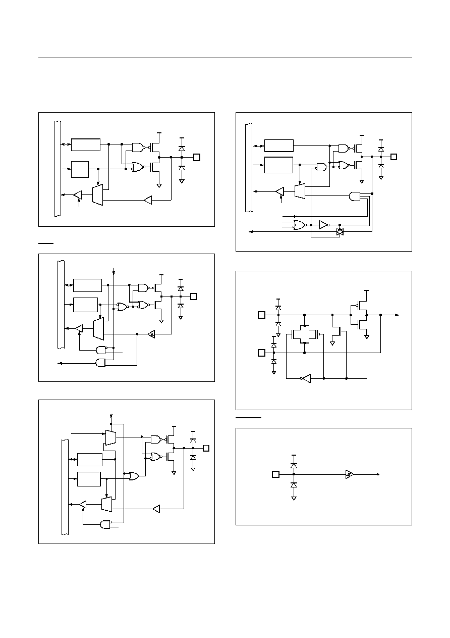
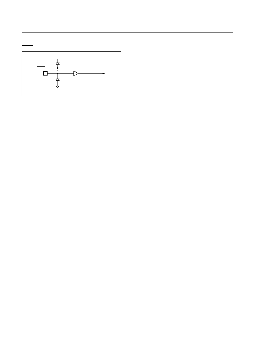
6. PORT STRUCTURES
R00~R07, R20~R27, R30~37
R40/INT0, R41/INT1, R42/INT2, R43/INT3, R44/
EC0
R54/WDTO, R55/BUZ
R64/AN7 ~ R67/AN7
X
IN
, X
OUT
RESET
Pin
Data Reg.
Dir.
Rd
V
DD
VSS
Reg.
Da
ta
Bu
s
M U X
M U X
D
a
ta
B
u
s
V
DD
V
SS
Pin
Data Reg.
Direction
Reg.
Rd
PMR Selection
Alternate Function
EX) INT0
M U X
Da
t
a
Bu
s
V
DD
V
SS
Pin
Data Reg.
Direction
Reg.
Rd
M U X
Selection
Secondary function
M U X
V
DD
V
SS
Pin
Da
ta
Bu
s
Data Reg.
Direction
Reg.
To A/D converter
Digital enable
Channel Sel.
A/D enable
Rd
XIN
V
DD
V
SS
XOUT
V
SS
Stop
RESET
V
DD
V
SS
HYUNDAI MicroElectronics
GMS82512/16/24
FEB. 2000 Ver 1.00
9
TEST
TEST
V
DD
V
SS
OTP version: disconnected
Mask version: connected
GMS82512/16/24
HYUNDAI MicroElectronics
10
FEB. 2000 Ver 1.00
7. ELECTRICAL CHARACTERISTICS
7.1 Absolute Maximum Ratings
Supply voltage ............................................. -0.3 to +7.0 V
Storage Temperature .................................. -40 to +125
°
C
Voltage on any pin with respect to Ground (V
SS
)
..................................................................-0.3 to V
DD
+0.3
Maximum current out of V
SS
pin .......................... 150 mA
Maximum current into V
DD
pin .............................. 80 mA
Maximum current sunk by (I
OL
per I/O Pin) .......... 20 mA
Maximum output current sourced by (I
OH
per I/O Pin)
................................................................................... 8 mA
Maximum current (
I
OL
) ...................................... 100 mA
Maximum current (
I
OH
)........................................ 50 mA
Note: Stresses above those listed under "Absolute Maxi-
mum Ratings" may cause permanent damage to the de-
vice. This is a stress rating only and functional operation of
the device at any other conditions above those indicated in
the operational sections of this specification is not implied.
Exposure to absolute maximum rating conditions for ex-
tended periods may affect device reliability.
7.2 Recommended Operating Conditions
7.3 A/D Converter Characteristics
(T
A
=25
°
C, V
SS
=0V, V
DD
=5.12V@f
XIN
=8MHz, V
DD
=3.072V@f
XIN
=4MHz)
Parameter
Symbol
Condition
Specifications
Unit
Min.
Max.
Supply Voltage
V
DD
f
XIN
=1 ~ 10 MHz
f
XIN
=1 ~ 8 MHz
f
XIN
=1 ~ 4 MHz
4.5
2.7
2.2
5.5
5.5
5.5
V
Operating Frequency
f
XIN
V
DD
=4.5~5.5V
V
DD
=2.7~5.5V
V
DD
=2.2~5.5V
1
1
1
10
8
4
MHz
Operating Temperature
T
OPR
Normal Version
Temperature Extention Version
-20
-40
85
85
°
C
Parameter
Symbol
Specifications
Unit
Min.
Typ.
1
Max.
f
XIN
=4MHz
f
XIN
=8MHz
Analog Input Voltage Range
V
AIN
V
SS
-
AV
DD
AV
DD
V
Non-linearity Error
N
NLE
-
±
1.0
±1.5
±1.5
LSB
Differential Non-linearity Error
N
DNLE
-
±
1.0
±1.5
±1.5
LSB
Zero Offset Error
N
ZOE
-
±
0.5
±1.5
±1.5
LSB
Full Scale Error
N
FSE
-
±
0.35
±0.5
±0.5
LSB
Gain Error
N
GE
-
±
1.0
±1.5
±1.5
LSB
Overall Accuracy
N
ACC
-
±
1.0
±1.5
±1.5
LSB
AV
DD
Input Current
I
REF
-
0.5
1.0
1.0
mA
Conversion Time
T
CONV
-
-
40
20
µ
s
HYUNDAI MicroElectronics
GMS82512/16/24
FEB. 2000 Ver 1.00
11
7.4 DC Electrical Characteristics
(T
A
=-20~85
°
C, V
DD
=2.7~5.5V, Ta= -20~85
°
C, f
XIN
=8MHz, V
SS
=0V)
,
Analog Power Supply Input Range
AV
DD
0.9V
DD
V
DD
1.1V
DD
V
1. Data in "Typ" column is at 25
°
C unless otherwise stated. These parameters are for design guidance only and are not tested.
Parameter
Symbol
Condition
Specifications
Unit
Min.
Typ.
1
1. Data in "Typ." column is at 4.5V, 25
°
C unless otherwise stated. These parameters are for design guidance only and are not tested.
Max.
Input High Voltage
V
IH1
V
DD
=4.5
V
DD
=2.7
X
IN
, RESET,
R4, R5, R6
0.8V
DD
-
V
DD
+0.3
V
V
IH2
R0, R2, R3
0.7V
DD
-
V
DD
+0.3
Input Low Voltage
V
IL1
V
DD
=4.5
V
DD
=2.7
X
IN
, RESET,
R4, R5, R6
-
0.2V
DD
V
V
IL2
R0, R2, R3
-
0.3V
DD
Output High Voltage
V
OH
V
DD
=4.5
V
DD
=2.7
I
OH1
=-2mA
R0,R2,R3,R4,R5
R6
V
DD
-1.0
-
-
V
Output Low Voltage
V
OL
V
DD
=4.5
V
DD
=2.7
I
OL1
=5mA
R0,R2,R3,R4,R5
R6
-
-
1.0
V
Power Fail Detect
Voltage
V
PFD
V
PFD
=3.0V
V
PFD
=2.4V
@ T
A
=25
°
C
0.9V
PFD
1.1V
PFD
V
Input High
Leakage Current
I
IH1
V
IN
=V
DD
All input pins
-5.0
-
5.0
µ
A
Input Low
Leakage Current
I
IL
V
IN
=V
SS
All input pins
-5.0
-
5.0
µ
A
Hysteresis
V
T+
, V
T-
RESET, EC0, SIN,
SCLK, INT0~INT3
0.3
0.8
V
Power Current
I
DD1
f
XIN
=8M H z
A ll input = V
S S
C rystal O scillator,
C
L1
=C
L2
=30pF@ 8M H z
-
8
20
mA
I
DD2
f
XIN
=4M H z
4
10
mA
I
STOP
A ll input = V
S S
-
1
10
µ
A
Parameter
Symbol
Specifications
Unit
Min.
Typ.
1
Max.
f
XIN
=4MHz
f
XIN
=8MHz
GMS82512/16/24
HYUNDAI MicroElectronics
12
FEB. 2000 Ver 1.00
7.5 AC Characteristics
(T
A
=-20~+85
°
C, V
DD
=5V
±
10%, V
SS
=0V)
Figure 7-1 Timing Chart
Parameter
Symbol
Pins
Specifications
Unit
Min.
Typ.
Max.
Operating Frequency
f
XIN
X
IN
1.0
-
10.0
MHz
Oscillation Stabilizing
Time
t
ST
X
IN
, X
OUT
-
-
20
ms
External Clock Pulse
Width
t
CPW
X
IN
40
-
-
ns
External Clock Transi-
tion Time
t
RCP,
t
FCP
X
IN
-
-
20
ns
Interrupt Pulse Width
t
IW
INT0, INT1, INT2, INT3
2
-
-
t
SYS
RESET Input Width
t
RST
RESET
8
-
-
t
SYS
Event Counter Input
Pulse Width
t
ECW
EC0
2
-
-
t
SYS
Event Counter Transi-
tion Time
t
REC,
t
FEC
EC0
-
-
20
ns
t
RCP
t
FCP
XIN
INT0~INT3
0.5V
V
DD
-0.5V
0.2V
DD
0.8V
DD
0.2V
DD
RESET
t
REC
t
FEC
0.2V
DD
0.8V
DD
EC0
t
IW
t
IW
t
RST
t
ECW
t
ECW
t
SYS
= 1/f
XIN
t
CPW
t
CPW
HYUNDAI MicroElectronics
GMS82512/16/24
FEB. 2000 Ver 1.00
13
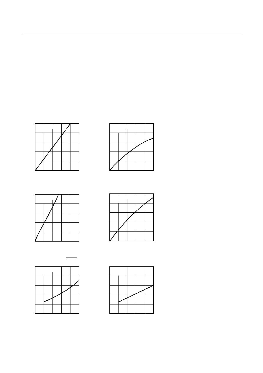
7.6 Typical Characteristic Curves
This graphs and tables provided in this section are for de-
sign guidance only and are not tested or guaranteed.
In some graphs or tables the data presented are out-
side specified operating range (e.g. outside specified
V
DD
range). This is for information only and devices
are guaranteed to operate properly only within the
specified range.
The data presented in this section is a statistical summary
of data collected on units from different lots over a period
of time. "Typical" represents the mean of the distribution
while "max" or "min" represents (mean + 3
) and (mean
-
3
) respectively where
is standard deviation
V
DD
-
V
IH2
4
3
2
1
0
(V)
V
IH2
2
3
4
5
6
V
DD
(V)
V
DD
-
V
IH1
4
3
2
1
0
(V)
V
IH1
2
3
4
5
6
V
DD
(V)
Ta=25
°
C
1
f
XIN
=8MHz
Ta=25
°
C
f
XIN
=8MHz
XIN, RESET,
R0, R2, R3 pins
I
OH
-
V
OH
-12
-9
-6
-3
0
0.3
0.6
0.9
1.2
1.5 (V)
Ta=25
°
C
V
DD
=4.5V
R0~R6 pins
(mA)
I
OH
V
DD
-V
OH
I
OL
-
V
OL1
20
15
10
5
0
(mA)
I
OL
0.2
0.4
0.6
0.8
1.0
V
OL
(V)
Ta=25
°
C
V
DD
=4.5V
R0~R6 pins
I
OH
-
V
OH
-12
-9
-6
-3
0
0.3
0.6
0.9
1.2
1.5 (V)
Ta=25
°
C
V
DD
=3.0V
R0~R6 pins
(mA)
I
OH
V
DD
-V
OH
I
OL
-
V
OL2
20
15
10
5
0
(mA)
I
OL
0.2
0.4
0.6
0.8
1.0
V
OL
(V)
Ta=25
°
C
V
DD
=3.0V
R0~R6 pins
R4, R5, R6 pins
GMS82512/16/24
HYUNDAI MicroElectronics
14
FEB. 2000 Ver 1.00
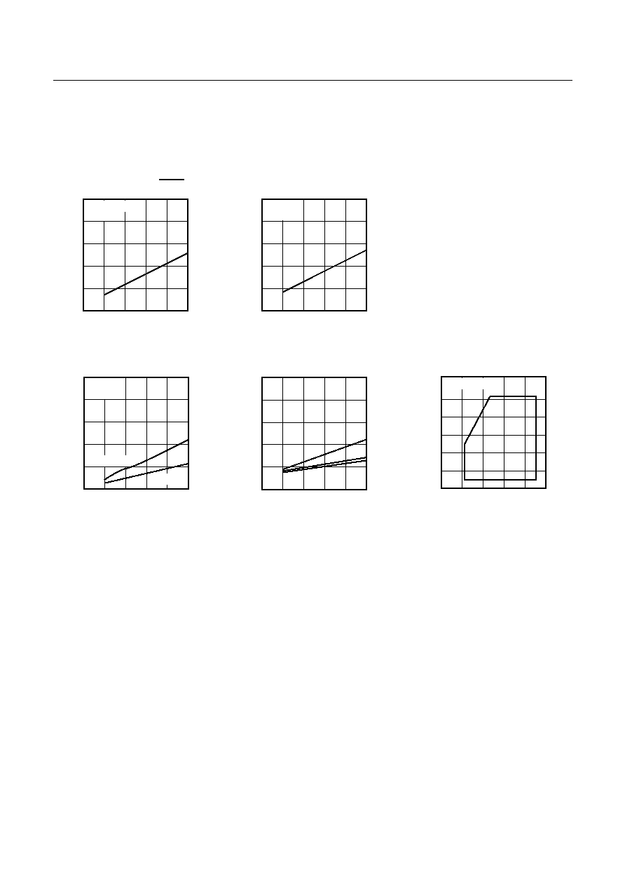
Ta= -20~85
°
C
Ta=25
°
C
I
DD
-
V
DD
20
15
10
5
0
(mA)
I
DD
2
3
4
5
6
V
DD
(V)
Normal Operation
10
6
4
2
0
(MHz)
f
XIN
2
3
4
5
6
V
DD
(V)
Operating Area
I
STOP
-
V
DD
0.4
0.3
0.2
0.1
0
(
µ
A)
I
DD
2
3
4
5
6
V
DD
(V)
Stop Mode
85
°
C
25
°
C
-20
°
C
f
XIN
= 8MHz
4MHz
V
DD
-
V
IL2
4
3
2
1
0
(V)
V
IL2
2
3
4
5
6
V
DD
(V)
V
DD
-
V
IL1
4
3
2
1
0
(V)
V
IL2
2
3
4
5
6
V
DD
(V)
Ta=25
°
C
1
f
XIN
=8MHz
Ta=25
°
C
f
XIN
=8MHz
R0, R2, R3 pins
8
XIN, RESET,
R4, R5, R6 pins
HYUNDAI MicroElectronics
GMS82512/16/24
FEB. 2000 Ver 1.00
15
8. MEMORY ORGANIZATION
The GMS82512/16/24 has separate address spaces for Pro-
gram memory and Data Memory. Program memory can
only be read, not written to. It can be up to 24K bytes of
Program memory. Data memory can be read and written to
up to 448 bytes including the stack area.
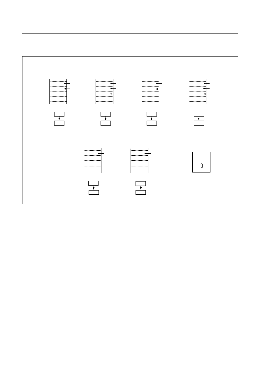
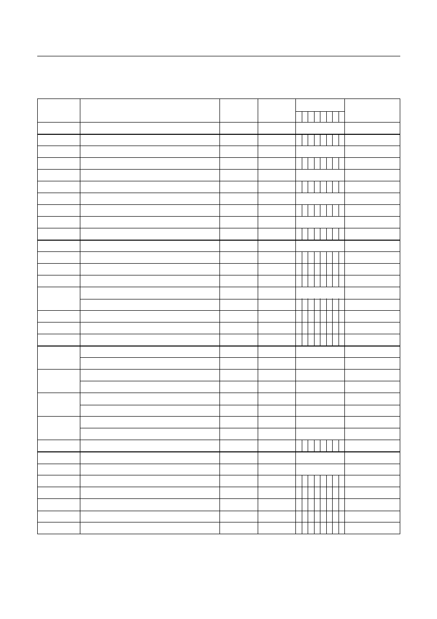
8.1 Registers
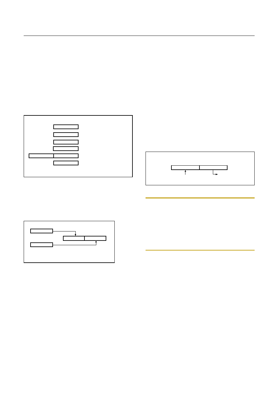
This device has six registers that are the Program Counter
(PC), a Accumulator (A), two index registers (X, Y), the
Stack Pointer (SP), and the Program Status Word (PSW).
The Program Counter consists of 16-bit register.
Figure 8-1 Configuration of Registers
Accumulator: The Accumulator is the 8-bit general pur-
pose register, used for data operation such as transfer, tem-
porary saving, and conditional judgement, etc.
The Accumulator can be used as a 16-bit register with Y
Register as shown below.
Figure 8-2 Configuration of YA 16-bit Register
X, Y Registers: In the addressing mode which uses these
index registers, the register contents are added to the spec-
ified address, which becomes the actual address. These
modes are extremely effective for referencing subroutine
tables and memory tables. The index registers also have in-
crement, decrement, comparison and data transfer func-
tions, and they can be used as simple accumulators.
Stack Pointer: The Stack Pointer is an 8-bit register used
for occurrence interrupts and calling out subroutines. Stack
Pointer identifies the location in the stack to be accessed
(save or restore).
Generally, SP is automatically updated when a subroutine
call is executed or an interrupt is accepted. However, if it
is used in excess of the stack area permitted by the data
memory allocating configuration, the user-processed data
may be lost.
The stack can be located at any position within 100
H
to
1FF
H
of the internal data memory. The SP is not initialized
by hardware, requiring to write the initial value (the loca-
tion with which the use of the stack starts) by using the ini-
tialization routine. Normally, the initial value of "FE
H
" is
used.
Note: The Stack Pointer must be initialized by software be-
cause its value is undefined after RESET.
Example: To initialize the SP
LDX
#0FEH
TXSP
; SP
FEH
Address 01FF
H
can not be used as stack. Don not use
1FF
H
, or malfunction would be occurred.
Program Counter: The Program Counter is a 16-bit wide
which consists of two 8-bit registers, PCH and PCL. This
counter indicates the address of the next instruction to be
executed. In reset state, the program counter has reset rou-
tine address (PC
H
:0FF
H
, PC
L
:0FE
H
).
Program Status Word: The Program Status Word (PSW)
contains several bits that reflect the current state of the
CPU. The PSW is described in Figure 8-3. It contains the
Negative flag, the Overflow flag, the Break flag the Half
Carry (for BCD operation), the Interrupt enable flag, the
Zero flag, and the Carry flag.
[Carry flag C]
This flag stores any carry or not borrow from the ALU of
CPU after an arithmetic operation and is also changed by
the Shift Instruction or Rotate Instruction.
ACCUMULATOR
X REGISTER
Y REGISTER
STACK POINTER
PROGRAM COUNTER
PROGRAM STATUS
WORD
X
A
SP
Y
PCL
PSW
PCH
Two 8-bit Registers can be used as a "YA" 16-bit Register
Y
A
Y
A
SP
01
H
Stack Address (100
H
~ 1FE
H
)
Bit 15
Bit 0
8 7
Hardware fixed
00
H
~FE
H
GMS82512/16/24
HYUNDAI MicroElectronics
16
FEB. 2000 Ver 1.00
[Zero flag Z]
This flag is set when the result of an arithmetic operation
or data transfer is "0" and is cleared by any other result.
Figure 8-3 PSW (Program Status Word) Register
[Interrupt disable flag I]
This flag enables/disables all interrupts except interrupt
caused by Reset or software BRK instruction. All inter-
rupts are disabled when cleared to "0". This flag immedi-
ately becomes "0" when an interrupt is served. It is set by
the EI instruction and cleared by the DI instruction.
[Half carry flag H]
After operation, this is set when there is a carry from bit 3
of ALU or there is no borrow from bit 4 of ALU. This bit
can not be set or cleared except CLRV instruction with
Overflow flag (V).
[Break flag B]
This flag is set by software BRK instruction to distinguish
BRK from TCALL instruction with the same vector ad-
dress.
[Direct page flag G]
This flag assigns RAM page for direct addressing mode. In
the direct addressing mode, addressing area is from zero
page 00
H
to 0FF
H
when this flag is "0". If it is set to "1",
addressing area is assigned 100
H
to 1FF
H
. It is set by
SETG instruction and cleared by CLRG.
[Overflow flag V]
This flag is set to "1" when an overflow occurs as the result
of an arithmetic operation involving signs. An overflow
occurs when the result of an addition or subtraction ex-
ceeds +127(7F
H
) or -128(80
H
). The CLRV instruction
clears the overflow flag. There is no set instruction. When
the BIT instruction is executed, bit 6 of memory is copied
to this flag.
[Negative flag N]
This flag is set to match the sign bit (bit 7) status of the re-
sult of a data or arithmetic operation. When the BIT in-
struction is executed, bit 7 of memory is copied to this flag.
N
NEGATIVE FLAG
V
G
B
H
I
Z
C
MSB
LSB
RESET VALUE: 00
H
PSW
OVERFLOW FLAG
BRK FLAG
CARRY FLAG RECEIVES
ZERO FLAG
INTERRUPT ENABLE FLAG
CARRY OUT
HALF CARRY FLAG RECEIVES
CARRY OUT FROM BIT 1 OF
ADDITION OPERLANDS
SELECT DIRECT PAGE
when G=1, page is selected to "page 1"
HYUNDAI MicroElectronics
GMS82512/16/24
FEB. 2000 Ver 1.00
17
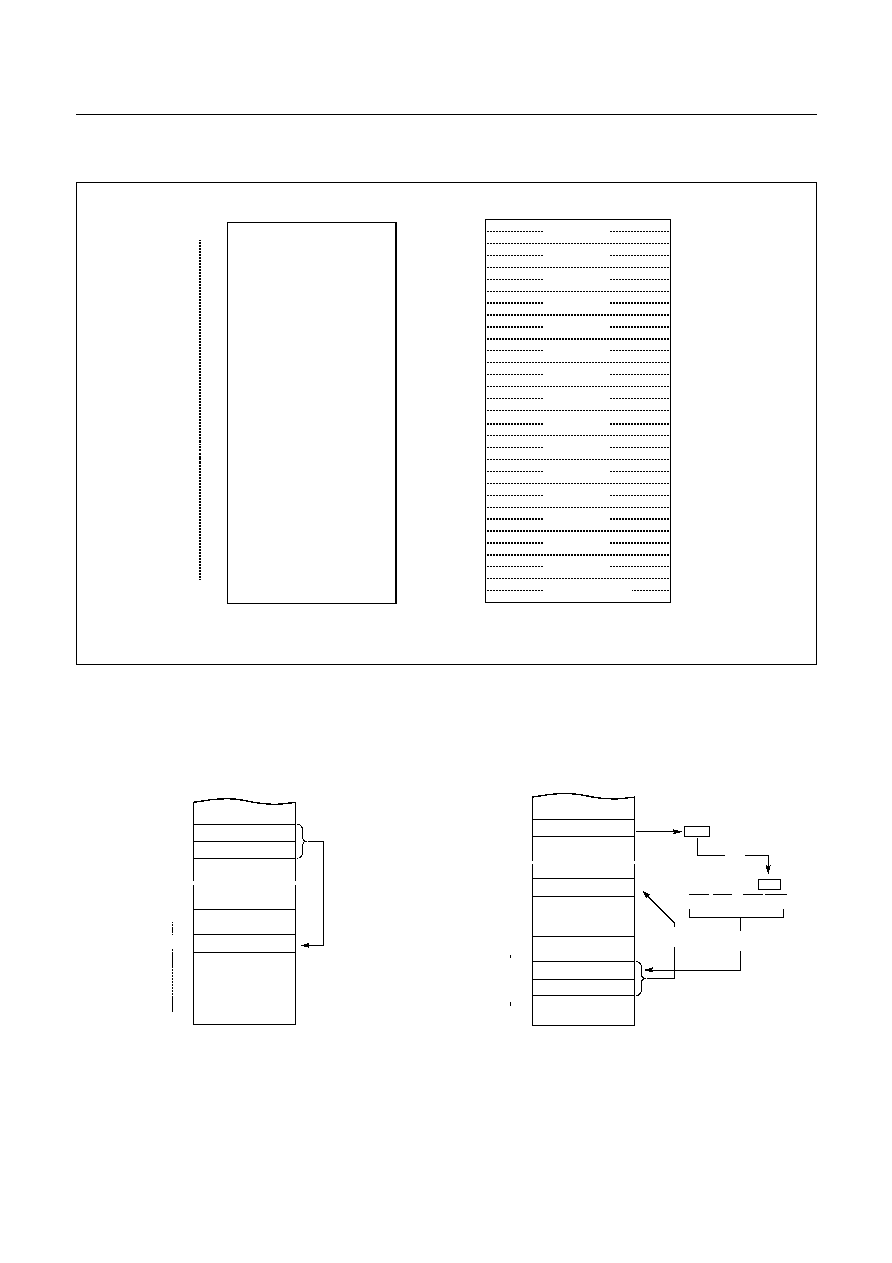
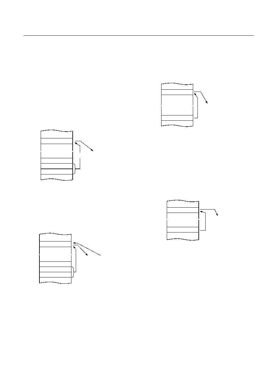
Figure 8-4 Stack Operation
At execution of
a CALL/TCALL/PCALL
PCL
PCH
01FB
SP after
execution
SP before
execution
01FC
01FC
01FD
01FE
01FE
Push
down
At acceptance
of interrupt
PCL
PCH
01FB
01FB
01FC
01FD
01FE
01FE
Push
down
PSW
At execution
of RET instruction
PCL
PCH
01FB
01FE
01FC
01FD
01FE
01FC
Pop
up
At execution
of RET instruction
PCL
PCH
01FB
01FE
01FC
01FD
01FE
01FB
Pop
up
PSW
0100H
01FEH
Stack
depth
At execution
of PUSH instruction
A
01FB
01FD
01FC
01FD
01FE
01FE
Push
down
SP after
execution
SP before
execution
PUSH A (X,Y,PSW)
At execution
of POP instruction
A
01FB
01FE
01FC
01FD
01FE
01FD
Pop
up
POP A (X,Y,PSW)
GMS82512/16/24
HYUNDAI MicroElectronics
18
FEB. 2000 Ver 1.00
8.2 Program Memory
A 16-bit program counter is capable of addressing up to
64K bytes, but this device has 24K bytes program memory
space only physically implemented. Accessing a location
above FFFF
H
will cause a wrap-around to 0000
H
.
Figure 8-5, shows a map of Program Memory. After reset,
the CPU begins execution from reset vector which is stored
in address FFFE
H
and FFFF
H
as shown in Figure 8-6.
As shown in Figure 8-5, each area is assigned a fixed loca-
tion in Program Memory. Program Memory area contains
the user program.
Figure 8-5 Program Memory Map
Page Call (PCALL) area contains subroutine program to
reduce program byte length by using 2 bytes PCALL in-
stead of 3 bytes CALL instruction. If it is frequently called,
it is more useful to save program byte length.
Table Call (TCALL) causes the CPU to jump to each
TCALL address, where it commences the execution of the
service routine. The Table Call service area spaces 2-byte
for every TCALL: 0FFC0
H
for TCALL15, 0FFC2
H
for
TCALL14, etc., as shown in Figure 8-7.
Example: Usage of TCALL
The interrupt causes the CPU to jump to specific location,
where it commences the execution of the service routine.
The External interrupt 0, for example, is assigned to loca-
tion 0FFFA
H
. The interrupt service locations spaces 2-byte
interval: 0FFF8
H
and 0FFF9
H
for External Interrupt 1,
0FFFA
H
and 0FFFB
H
for External Interrupt 0, etc.
Any area from 0FF00
H
to 0FFFF
H
, if it is not going to be
used, its service location is available as general purpose
Program Memory.
Figure 8-6 Interrupt Vector Area
Interrupt
Vector Area
C000
H
FEFF
H
FF00
H
FFC0
H
FFDF
H
FFE0
H
FFFF
H
P
C
A
L
L
ar
ea
D000
H
A000
H
TCALL area
GM
S
82512
,
12K
ROM
GM
S
82516
,
16K
R
O
M
GM
S
8252
4,
24K
ROM
0FFE0H
E2
Address
Vector Area Memory
E4
E6
E8
EA
EC
EE
F0
F2
F4
F6
F8
FA
FC
FE
-
-
-
Basic Interval Timer
-
-
-
External Interrupt 2
Timer/Counter 1 Interrupt
External Interrupt 0
-
RESET Vector Area
External Interrupt 1
Watchdog Timer Interrupt
"-" means reserved area.
NOTE:
Timer/Counter 2 Interrupt
External Interrupt 3
Timer/Counter 0 Interrupt
Timer/Counter 3 Interrupt
A/D Converter
HYUNDAI MicroElectronics
GMS82512/16/24
FEB. 2000 Ver 1.00
19
Figure 8-7 PCALL and TCALL Memory Area
PCALL
rel
4F35
PCALL
35H
TCALL
n
4A
TCALL 4
0FFC0
H
C1
Address
Program Memory
C2
C3
C4
C5
C6
C7
C8
0FF00
H
Address
PCALL Area Memory
0FFFF
H
PCALL Area
(256 Bytes)
* means that the BRK software interrupt is using
same address with TCALL0.
NOTE:
TCALL 15
TCALL 14
TCALL 13
TCALL 12
TCALL 11
TCALL 10
TCALL 9
TCALL 8
TCALL 7
TCALL 6
TCALL 5
TCALL 4
TCALL 3
TCALL 2
TCALL 1
TCALL 0 / BRK *
C9
CA
CB
CC
CD
CE
CF
D0
D1
D2
D3
D4
D5
D6
D7
D8
D9
DA
DB
DC
DD
DE
DF
4F
~
~
~
~
NEXT
35
0FF35
H
0FF00
H
0FFFF
H
11111111 11010110
01001010
PC:
FH
FH
DH 6H
4A
~
~
~
~
25
0FFD6
H
0FF00
H
0FFFF
H
D1
NEXT
0FFD7
H
0D125
H
Reverse

GMS82512/16/24
HYUNDAI MicroElectronics
20
FEB. 2000 Ver 1.00
Example: The usage software example of Vector address for GMS82524.
ORG
0FFE0H
DW
NOT_USED
DW
NOT_USED
DW
NOT_USED
DW
BIT_TIMER
; Basic Interval Timer
DW
WD_TIMER
; Watchdog Timer
DW
ADC
; ADC
DW
TIMER3
; Timer-3
DW
TIMER2
; Timer-2
DW
TIMER1
; Timer-1
DW
TIMER0
; Timer-0
DW
INT3
; Int.3
DW
INT2
; Int.2
DW
INT1
; Int.1
DW
INT0
; Int.0
DW
NOT_USED
; -
DW
RESET
; Reset
ORG
0A000H
; 24K ROM Start address
;
ORG
0C000H
; 16K ROM Start address
;
ORG
0D000H
; 12K ROM Start address
;*******************************************
;
MAIN PROGRAM
*
;*******************************************
;
RESET:
DI
;Disable All Interrupts
CLRG
LDX
#0
RAM_CLR: LDA
#0
;RAM Clear(!0000H->!00BFH)
STA
{X}+
CMPX
#0C0H
BNE
RAM_CLR
;
LDX
#0FEH
;Stack Pointer Initialize
TXSP
;
LDM
R0, #0
;Normal Port 0
LDM
R0DD,#82H
;Normal Port Direction
:
:
:
LDM
TDR0,#250
;8us x 250 = 2000us
LDM
TM0,#1FH
;Start Timer0, 8us at 8MHz
LDM
IRQH,#0
LDM
IRQL,#0
LDM
IENH,#0C8H
;Enable Timer0, INT0, INT1
LDM
IENL,#0
LDM
IEDS,#55H
;Select falling edge detect on INT pin
LDM
PMR4,#3H
;Set external interrupt pin(INT0, INT1)
EI
;Enable master interrupt
:
:
:
:
:
NOT_USED:NOP
RETI
HYUNDAI MicroElectronics
GMS82512/16/24
FEB. 2000 Ver 1.00
21
8.3 Data Memory
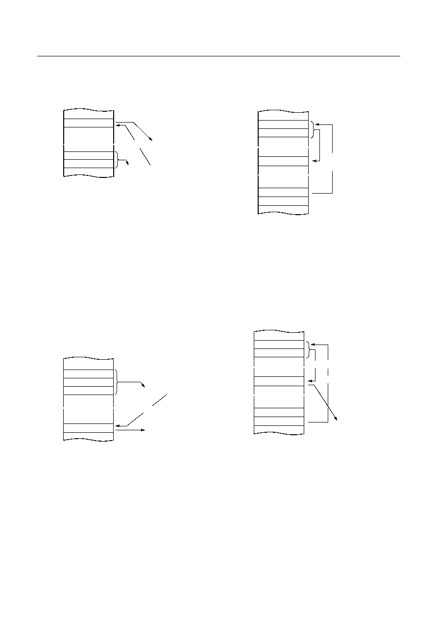
Figure 8-8 shows the internal Data Memory space availa-
ble. Data Memory is divided into four groups, a user RAM,
control registers, Stack, and LCD memory.
Figure 8-8 Data Memory Map
User Memory
The GMS825xx has 448
×
8 bits for the user memory
(RAM).
Control Registers
The control registers are used by the CPU and Peripheral
function blocks for controlling the desired operation of the
device. Therefore these registers contain control and status
bits for the interrupt system, the timer/ counters, analog to
digital converters and I/O ports. The control registers are in
address range of 0C0
H
to 0FF
H
.
Note that unoccupied addresses may not be implemented
on the chip. Read accesses to these addresses will in gen-
eral return random data, and write accesses will have an in-
determinate effect.
More detailed informations of each register are explained
in each peripheral section.
Note: Write only registers can not be accessed by bit ma-
nipulation instruction. Do not use read-modify-write instruc-
tion. Use byte manipulation instruction, for example "LDM".
Example; To write at CKCTLR
LDM
CLCTLR,#09H
;Divide ratio(
÷
32)
Stack Area
The stack provides the area where the return address is
saved before a jump is performed during the processing
routine at the execution of a subroutine call instruction or
the acceptance of an interrupt.
When returning from the processing routine, executing the
subroutine return instruction [RET] restores the contents of
the program counter from the stack; executing the interrupt
return instruction [RETI] restores the contents of the pro-
gram counter and flags.
The save/restore locations in the stack are determined by
the stack pointed (SP). The SP is automatically decreased
after the saving, and increased before the restoring. This
means the value of the SP indicates the stack location
number for the next save. Refer to Figure 8-4 on page 17.
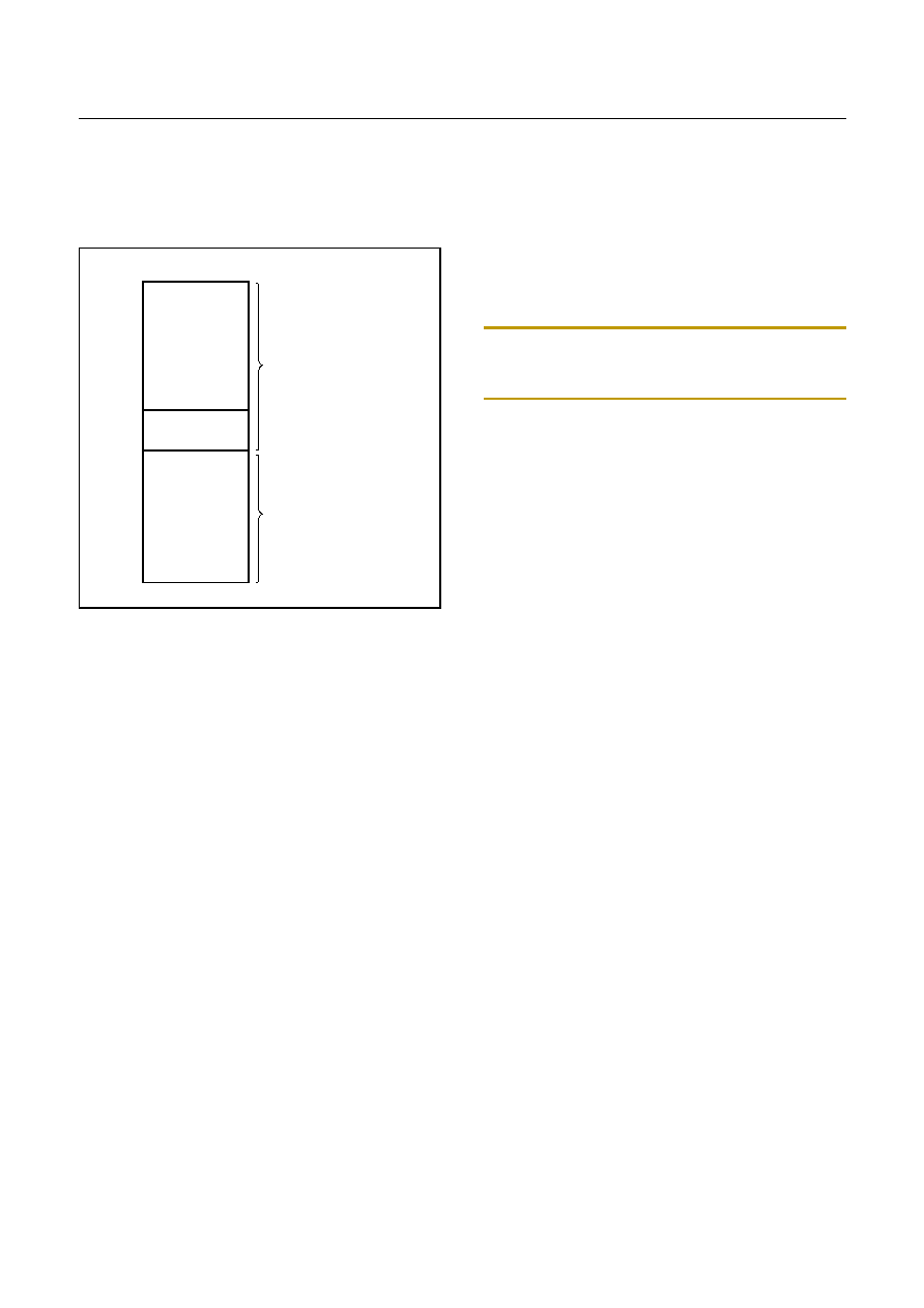
User Memory
Control
Registers
or Stack Area
0000
H
00BF
H
00C0
H
00FF
H
0100
H
01FF
H
PAGE0
User Memory
PAGE1
When "G-flag=0",
When "G-flag=1"
this page is selected
GMS82512/16/24
HYUNDAI MicroElectronics
22
FEB. 2000 Ver 1.00
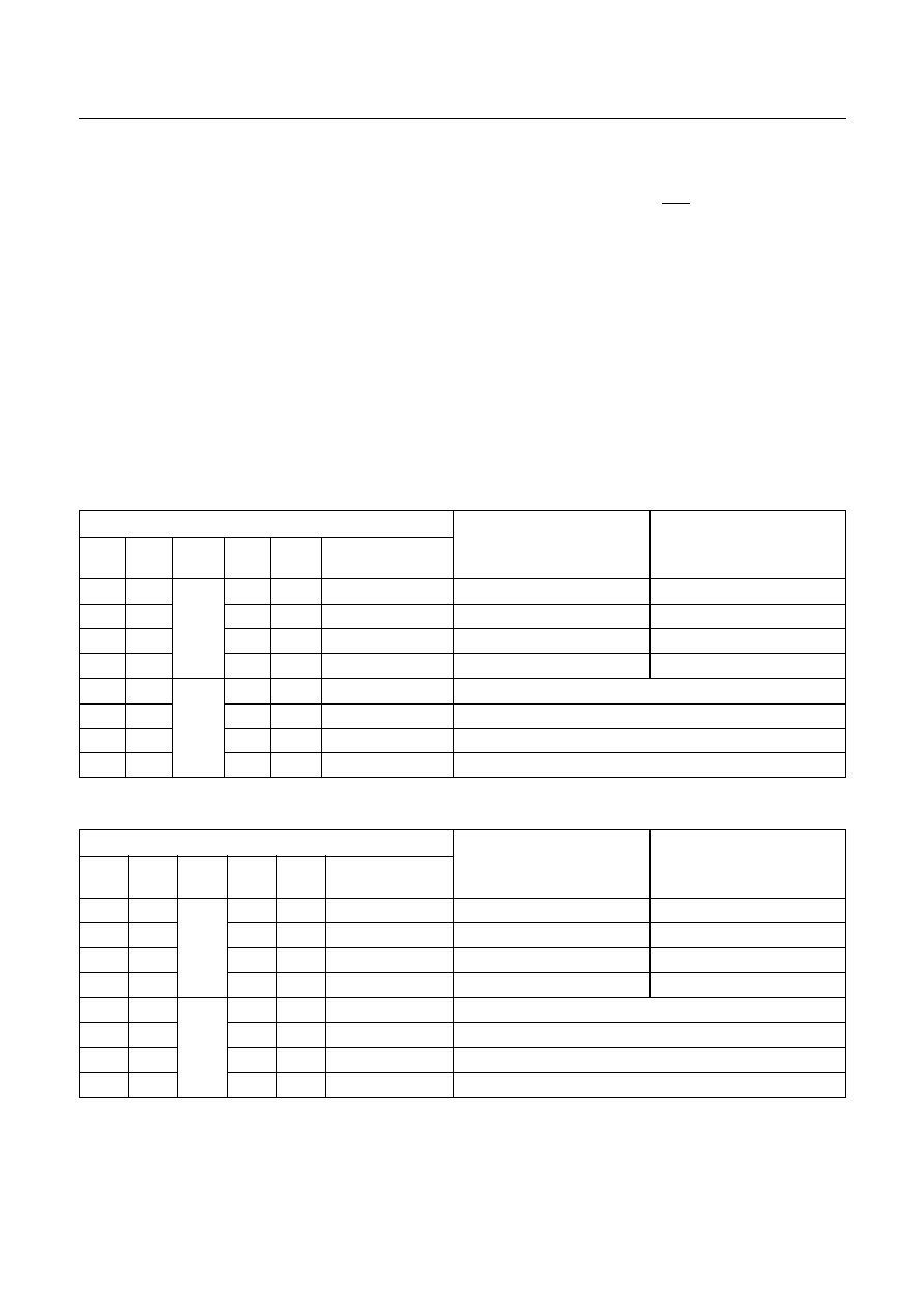
Address
Register Name
Symbol
R/W
Initial Value
Page
7 6 5 4 3 2 1 0
00C0
R0 port data register
R0
R/W
Undefined
page 28
00C1
R0 port I/O direction register
R0DD
W
0 0 0 0 0 0 0 0
page 28
00C4
R2 port data register
R2
R/W
Undefined
page 28
00C5
R2 port I/O direction register
R2DD
W
0 0 0 0 0 0 0 0
page 28
00C6
R3 port data register
R3
R/W
Undefined
page 28
00C7
R3 port I/O direction register
R3DD
W
0 0 0 0 0 0 0 0
page 28
00C8
R4 port data register
R4
R/W
Undefined
page 29
00C9
R4 port I/O direction register
R4DD
W
- - - 0 0 0 0 0
page 29
00CA
R5 port data register
R5
R/W
Undefined
page 30
00CB
R5 port I/O direction register
R5DD
W
- - 0 0 - - - -
page 30
00CC
R6 port data register
R6
R/W
Undefined
page 30
00CD
R6 port I/O direction register
R6DD
W
0 0 0 0 - - - -
page 30
00D0
R4 port mode register
PMR4
W
- - - 0 0 0 0 0
page 29, page 53
00D1
R5 port mode register
PMR5
W
- - 0 0 - - - -
page 30, page 45
00D3
Basic interval timer mode register
BITR
R
Undefined
page 32
Clock control register
CKCTLR
W
- - 0 1 0 1 1 1
page 32
00E0
Watchdog Timer Register
WDTR
W
- 0 1 1 1 1 1 1
page 54
00E2
Timer mode register 0
TM0
R/W
0 0 0 0 0 0 0 0
page 34
00E3
Timer mode register 2
TM2
R/W
0 0 0 0 0 0 0 0
page 34
00E4
Timer 0 data register
TDR0
W
Undefined
page 34
Timer 0 counter register
T0
R
Undefined
page 34
00E5
Timer 1 data register
TDR1
W
Undefined
page 34
Timer 1 counter register
T1
R
Undefined
page 34
00E6
Timer 2 data register
TDR2
W
Undefined
page 34
Timer 2 counter register
T2
R
Undefined
page 34
00E7
Timer 3 data register
TDR3
W
Undefined
page 34
Timer 3 counter register
T3
R
Undefined
page 34
00E8
A/D converter mode register
ADCM
R/W
- - 0 0 0 0 0 1
page 44
00E9
A/D converter data register
ADR
R
Undefined
page 44
00EC
Buzzer driver register
BUR
W
Undefined
page 45
00F4
Interrupt enable register low
IENL
R/W
0 0 0 - - - - -
page 48
00F5
Interrupt request flag register low
IRQL
R/W
0 0 0 - - - - -
page 47
00F6
Interrupt enable register high
IENH
R/W
0 0 0 0 0 0 0 0
page 48
00F7
Interrupt request flag register high
IRQH
R/W
0 0 0 0 0 0 0 0
page 47
00F8
External interrupt edge selection register
IEDS
W
0 0 0 0 0 0 0 0
page 53
Table 8-1 Control Registers
HYUNDAI MicroElectronics
GMS82512/16/24
FEB. 2000 Ver 1.00
23
00F9
Power fail detection register
PFDR
R/W
- - - - 1 1 0 0
page 61
Address
Register Name
Symbol
R/W
Initial Value
Page
7 6 5 4 3 2 1 0
Table 8-1 Control Registers
Registers are controlled by byte manipulation instruction such as LDM etc., do not use bit manipulation
W
Registers are controlled by both bit and byte manipulation instruction.
R/W
instruction such as SET1, CLR1 etc. If bit manipulation instruction is used on these registers,
content of other seven bits are may varied to unwanted value.
- : this bit location is reserved.

GMS82512/16/24
HYUNDAI MicroElectronics
24
FEB. 2000 Ver 1.00
8.4 Addressing Mode
The GMS800 series MCU uses six addressing modes;
· Register addressing
· Immediate addressing
· Direct page addressing
· Absolute addressing
· Indexed addressing
· Register-indirect addressing
(1) Register Addressing
Register addressing accesses the A, X, Y, C and PSW.
(2) Immediate Addressing
#imm
In this mode, second byte (operand) is accessed as a data
immediately.
Example:
0435
ADC
#35H
When G-flag is 1, then RAM address is defined by 16-bit
address which is composed of 8-bit RAM paging register
(RPR) and 8-bit immediate data.
Example: G=1
E45535
LDM
35H,#55H
(3) Direct Page Addressing
dp
In this mode, a address is specified within direct page.
Example; G=0
C535
LDA
35H
;A
RAM[35H]
35
A+35H+C
A
04
MEMORY
E4
0F100H
data ¨ 55H
~
~
~
~
data
0135H
35
0F102H
55
0F101H
data
35
35H
0E551H
data
A
~
~
~
~
C5
0E550H
HYUNDAI MicroElectronics
GMS82512/16/24
FEB. 2000 Ver 1.00
25
(4) Absolute Addressing
!abs
Absolute addressing sets corresponding memory data to
Data, i.e. second byte (Operand I) of command becomes
lower level address and third byte (Operand II) becomes
upper level address.
With 3 bytes command, it is possible to access to whole
memory area.
ADC, AND, CMP, CMPX, CMPY, EOR, LDA, LDX,
LDY, OR, SBC, STA, STX, STY
Example;
0735F0
ADC
!0F035H
;A
ROM[0F035H]
The operation within data memory (RAM)
ASL, BIT, DEC, INC, LSR, ROL, ROR
Example; Addressing accesses the address 0135
H
regard-
less of G-flag.
983501
INC
!0135H
;A
ROM[135H]
(5) Indexed Addressing
X indexed direct page (no offset)
{X}
In this mode, a address is specified by the X register.
ADC, AND, CMP, EOR, LDA, OR, SBC, STA, XMA
Example; X=15
H
, G=1
D4
LDA
{X}
;ACC
RAM[X].
X indexed direct page, auto increment
{X}+
In this mode, a address is specified within direct page by
the X register and the content of X is increased by 1.
LDA, STA
Example; G=0, X=35
H
DB
LDA
{X}+
X indexed direct page (8 bit offset)
dp+X
This address value is the second byte (Operand) of com-
mand plus the data of
-register. And it assigns the mem-
ory in Direct page.
ADC, AND, CMP, EOR, LDA, LDY, OR, SBC, STA
STY, XMA, ASL, DEC, INC, LSR, ROL, ROR
Example; G=0, X=0F5
H
07
0F100H
~
~
~
~
data
0F035H
F0
0F102H
35
0F101H
A+data+C
A
address: 0F035
98
0F100H
~
~
~
~
data
135H
01
0F102H
35
0F101H
data+1
data
address: 0135
data
D4
115H
0E550H
data
A
~
~
~
~
data
DB
35H
data Æ A
~
~
~
~
36H Æ X
GMS82512/16/24
HYUNDAI MicroElectronics
26
FEB. 2000 Ver 1.00
C645
LDA
45H+X
Y indexed direct page (8 bit offset)
dp+Y
This address value is the second byte (Operand) of com-
mand plus the data of Y-register, which assigns Memory in
Direct page.
This is same with above (2). Use Y register instead of X.
Y indexed absolute
!abs+Y
Sets the value of 16-bit absolute address plus Y-register
data as Memory.This addressing mode can specify memo-
ry in whole area.
Example; Y=55
H
D500FA
LDA
!0FA00H+Y
(6) Indirect Addressing
Direct page indirect
[dp]
Assigns data address to use for accomplishing command
which sets memory data (or pair memory) by Operand.
Also index can be used with Index register X,Y.
JMP, CALL
Example; G=0
3F35
JMP
[35H]
X indexed indirect
[dp+X]
Processes memory data as Data, assigned by 16-bit pair
m e m o r y w h i c h i s d e t e r m i n e d b y p a i r d a t a
[dp+X+1][dp+X] Operand plus
X-register data in Direct
page.
ADC, AND, CMP, EOR, LDA, OR, SBC, STA
Example; G=0, X=10
H
1625
ADC
[25H+X]
Y indexed indirect
[dp]+Y
Processes memory data as Data, assigned by the data
[dp+1][dp] of 16-bit pair memory paired by Operand in Di-
rect page
plus Y-register data.
ADC, AND, CMP, EOR, LDA, OR, SBC, STA
Example; G=0, Y=10
H
data
45
3AH
0E551H
data
A
~
~
~
~
C6
0E550H
45H+0F5H=13AH
D5
0F100H
data
A
~
~
~
~
data
0FA55H
0FA00H+55H=0FA55H
FA
0F102H
00
0F101H
0A
35H
jump to
~
~
~
~
35
0FA00H
E3
36H
3F
0E30AH
NEXT
~
~
~
~
address 0E30AH
05
35H
0E005H
~
~
~
~
25
0FA00H
E0
36H
16
0E005H
data
~
~
~
~
A + data + C
A
25 + X(10) = 35H
HYUNDAI MicroElectronics
GMS82512/16/24
FEB. 2000 Ver 1.00
27
1725
ADC
[25H]+Y
Absolute indirect
[!abs]
The program jumps to address specified by 16-bit absolute
address.
JMP
Example; G=0
1F25E0
JMP
[!0C025H]
05
25H
0E005H + Y(10)
~
~
~
~
25
0FA00H
E0
26H
17
0E015H
data
~
~
~
~
= 0E015H
A + data + C
A
25
0E025H
jump to
~
~
~
~
E0
0FA00H
E7
0E026H
25
0E725H
NEXT
~
~
~
~
1F
PROGRAM MEMORY
address 0E30AH
GMS82512/16/24
HYUNDAI MicroElectronics
28
FEB. 2000 Ver 1.00
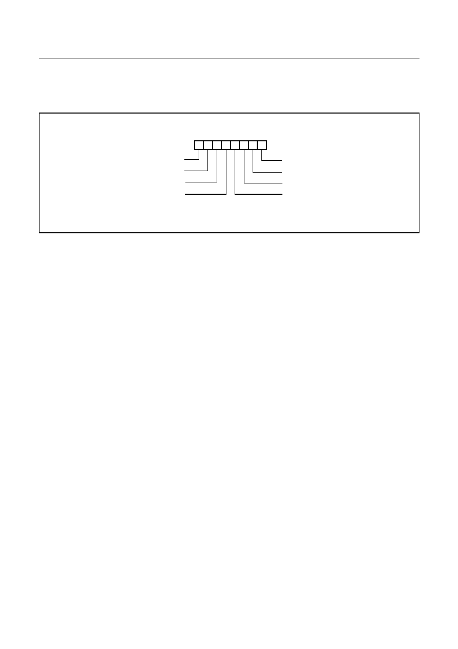
9. I/O PORTS
The GMS825xx has six ports (R0, R2, R3, R4, R5, and
R6).These ports pins may be multiplexed with an alternate
function for the peripheral features on the device.
All pins have data direction registers which can define
these ports as output or input. A "1" in the port direction
register configure the corresponding port pin as output.
Conversely, write "0" to the corresponding bit to specify it
as input pin. For example, to use the even numbered bit of
R0 as output ports and the odd numbered bits as input
ports, write "55
H
" to address 0C1
H
(R0 port direction reg-
ister) during initial setting as shown in Figure 9-1.
All the port direction registers in the GMS825xx have 0
written to them by reset function. On the other hand, its in-
itial status is input.
Figure 9-1 Example of port I/O assignment
R0 and R0DD register: R0 is an 8-bit CMOS bidirection-
al I/O port (address 0C0
H
). Each I/O pin can independently
used as an input or an output through the R0DD register
(address 0C1
H
).
R2 and R2DD register: R2 is an 8-bit CMOS bidirection-
al I/O port (address 0C4
H
). Each I/O pin can independently
used as an input or an output through the R2DD register
(address 0C5
H
).
R3 and R3DD register: R3 is an 8-bit CMOS bidirection-
al I/O port (address 0C6
H
). Each I/O pin can independently
used as an input or an output through the R3DD register
(address 0C7
H
).
I: INPUT PORT
WRITE "55
H
" TO PORT R0 DIRECTION REGISTER
0 1 0 1 0 1 0 1
I O I O I O I O
R0 data
R1 data
R0 direction
R1 direction
0C0
H
0C1
H
0C2
H
0C3
H
7 6 5 4 3 2 1 0
BIT
7 6 5 4 3 2 1 0
PORT
O: OUTPUT PORT
R0 Data Register
R0
ADDRESS: 0C0
H
RESET VALUE: Undefined
R07 R06 R05 R04 R03 R02 R01 R00
Port Direction
R0 Direction Register
R0DD
ADDRESS: 0C1
H
RESET VALUE: 00
H
0: Input
1: Output
Input / Output data
R2 Data Register
R2
ADDRESS: 0C4
H
RESET VALUE: Undefined
R27 R26 R25 R24 R23 R22 R21 R20
Port Direction
R2 Direction Register
R2DD
ADDRESS: 0C5
H
RESET VALUE: 00
H
0: Input
1: Output
Input / Output data
R3 Data Register
R3
ADDRESS: 0C6
H
RESET VALUE: Undefined
R37 R36 R35 R34 R33 R32 R31 R30
Port Direction
R3 Direction Register
R3DD
ADDRESS: 0C7
H
RESET VALUE: 00
H
0: Input
1: Output
Input / Output data
HYUNDAI MicroElectronics
GMS82512/16/24
FEB. 2000 Ver 1.00
29
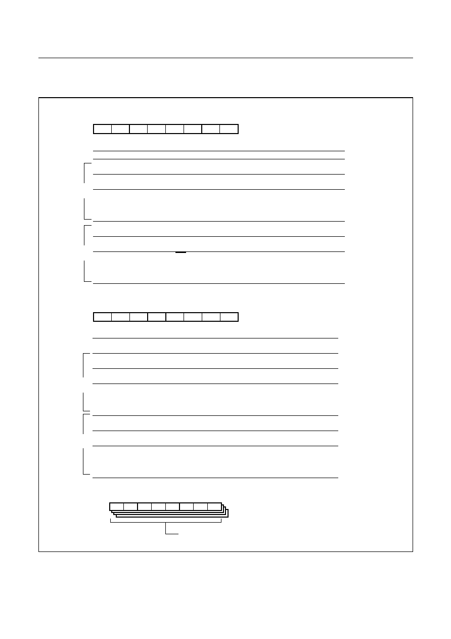
R4 and R4DD register: R4 is an 5-bit CMOS bidirection-
al I/O port (address 0C8
H
). Each I/O pin can independently
used as an input or an output through the R4DD register
(address 0C9
H
).
In addition, Port R4 is multiplexed with various special
features. The control register PMR4 (address 0D0
H
) con-
trols the selection of alternate function. After reset, this
value is "0", port may be used as normal I/O port.
To use alternate function such as external interrupt or ex-
ternal counter input, write "1" in the corresponding bit of
PMR4.
Regardless of the direction register R4DD, PMR4 is select-
ed to use as alternate functions, port pin can be used as a
corresponding alternate features.
R4 Port Mode Register
PMR4
ADDRESS: 0D0
H
RESET VALUE: 00
H
0: R40
1: INT0
0
0: R41
1: INT1
0: R42
1: INT2
0: R43
1: INT3
0: R44
1: EC0
1
2
3
4
Edge Selection Register
IEDS
ADDRESS: 0F8H
RESET VALUE: 00H
0
1
2
3
4
5
6
7
INT0
INT1
INT2
INT3
External Interrupt Edge Select
00: Reserved
01: Falling (1-to-0 transition)
10: Rising (0-to-1 transition)
11: Both (Rising & Falling)
R4 Data Register
R4
ADDRESS: 0C8
H
RESET VALUE: Undefined
-
-
-
R44 R43 R42 R41 R40
Port Direction
R4 Direction Register
R4DD
ADDRESS: 0C9
H
RESET VALUE: 00
H
0: Input
1: Output
Input / Output data
-
-
-
-
-
-
Port Pin
Alternate Function
R40
R41
R42
R43
R44
INT0 (External Interrupt 0)
INT1 (External Interrupt 1)
INT2 (External Interrupt 2)
INT3 (External Interrupt 3)
EC0 (External count input to Timer/
Counter 0)
GMS82512/16/24
HYUNDAI MicroElectronics
30
FEB. 2000 Ver 1.00
R5 and R5DD register: R5 is an 2-bit CMOS bidirection-
al I/O port (address 0CA
H
). Each I/O pin can independent-
ly used as an input or an output through the R5DD register
(address 0CB
H
).
The control register PMR5 (address D1
H
) controls the se-
lection alternate function. After reset, this value is "0", port
may be used as general I/O ports. To use buzzer function,
write "1" to the PMR5 and the pin R55 must be defined as
output mode (the bit 5 of R5DD=1)
R6 and R6DD register: R6 is an 4-bit CMOS bidirection-
al I/O port (address 0CC
H
). Each I/O pin can independent-
ly used as an input or an output through the R6DD register
(address 0CD
H
).
R6DD (address CD
H
) controls the direction of the R6 pins,
even when they are being used as analog inputs. The user
must make sure to keep the pins configured as inputs when
using them as analog inputs.
Port Pin
Alternate Function
R54
R55
WDTO (Watchdog timer output)
BUZ (Square-wave output for buzzer)
R5 Port Mode Register
PMR5
ADDRESS: 0D1
H
RESET VALUE: --00----
B
-
-
-
-
R54/WDTO Selection
BUZ
-
-
0: R54
1: WDTO (Output)
R55/BUZ Selection
0: R55
1: BUZ (Output)
W DTO
R5 Data Register
R5
ADDRESS: 0CA
H
RESET VALUE: Undefined
-
-
R55 R54 -
-
-
-
Port Direction
R5 Direction Register
R5DD
ADDRESS: 0CB
H
RESET VALUE: 00
H
0: Input
1: Output
Input / Output data
-
-
-
-
-
-
Port Pin
Alternate Function
R64
R65
R66
R67
AN4 (ADC input 4)
AN5 (ADC input 5)
AN6 (ADC input 6)
AN7 (ADC input 7)
R6 Data Register
R6
ADDRESS: 0CC
H
RESET VALUE: Undefined
R67 R66 R65 R64
Port Direction
R6 Direction Register
R6DD
ADDRESS: 0CD
H
RESET VALUE: 0000----
B
0: Input
1: Output
Input / Output data
-
-
-
-
-
-
-
-
HYUNDAI MicroElectronics
GMS82512/16/24
FEB. 2000 Ver 1.00
31
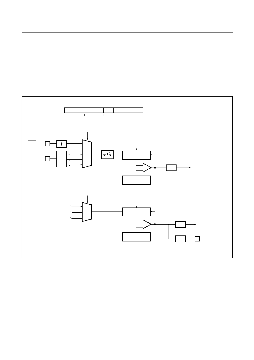
10. BASIC INTERVAL TIMER
The GMS825xx has one 8-bit Basic Interval Timer that is
free-run and can not stop. Block diagram is shown in Fig-
ure 10-1.
In addition, the Basic Interval Timer generates the time
base for watchdog timer counting. It also provides a Basic
interval timer interrupt (BITIF). As the count overflow
from FF
H
to 00
H
, this overflow causes the interrupt to be
generated. The Basic Interval Timer is controlled by the
clock control register (CKCTLR) shown in Figure 10-2.
Source clock can be selected by lower 3 bits of CKCTLR.
BITR and CKCTLR are located at same address, and ad-
dress 0D3
H
is read as a BITR, and written to CKCTLR.
Figure 10-1 Block Diagram of Basic Interval Timer
Table 10-1 Basic Interval Timer Interrupt Time
MUX
Basic Interval Timer Interrupt
BITR
Select Input clock 3
Basic Interval Timer
source
clock
8-bit up-counter
BTS[2:0]
BTCL
÷
2048
÷
1024
÷
512
÷
256
÷
128
÷
64
÷
32
÷
16
To Watchdog timer (WDTCK)
CKCTLR
clear
overflow
Internal bus line
clock control register
[0D3
H
]
[0F9
H
]
BITIF
Read
X
IN
PIN
Prescal
e
r
CKCTLR
[2:0]
Source clock
Interrupt (overflow) Period (ms)
@ f
XIN
= 8MHz
000
001
010
011
100
101
110
111
f
XIN
÷
16
f
XIN
÷
32
f
XIN
÷
64
f
XIN
÷
128
f
XIN
÷
256
f
XIN
÷
512
f
XIN
÷
1024
f
XIN
÷
2048
0.512
1.024
2.048
4.096
8.192
16.384
32.768
65.536
GMS82512/16/24
HYUNDAI MicroElectronics
32
FEB. 2000 Ver 1.00
Figure 10-2 BITR: Basic Interval Timer Mode Register
Example 1:
Interrupt request flag is generated every 8.192ms at 4MHz.
:
LDM
CKCTLR,#1BH
SET1
BITE
EI
:
Example 2:
Interrupt request flag is generated every 8.192ms at 8MHz.
:
LDM
CKCTLR,#1CH
SET1
BITE
EI
:
BTCL
7
6
5
4
3
2
1
0
WDTON
-
-
BTS1
Basic Interval Timer source clock select
000: f
XIN
÷
16
001: f
XIN
÷
32
010: f
XIN
÷
64
011: f
XIN
÷
128
100: f
XIN
÷
256
101: f
XIN
÷
512
110: f
XIN
÷
1024
111: f
XIN
÷
2048
Clear bit
0: Normal operation (free-run)
1: Clear 8-bit counter (BITR) to "0". This bit becomes 0 automatically
INITIAL VALUE: --01 0111
B
ADDRESS: 0D3
H
after one machine cycle, and starts counting.
CKCTLR
INITIAL VALUE: Undefined
ADDRESS: 0D3
H
BITR
Both register are in same address,
when write, to be a CKCTLR,
when read, to be a BITR.
Caution:
8-BIT FREE-RUN BINARY COUNTER
ENPCK
BTS0
BTS2
BTCL
BTCL
7
6
5
4
3
2
1
0
Enable Peripheral clock
If this bit is 0, all peripherals are disabled such as Timer, ADC, PWM, etc.
0: Operate as a 6-bit general timer
1: Enable Watchdog Timer operation
See the section "Watchdog Timer".
HYUNDAI MicroElectronics
GMS82512/16/24
FEB. 2000 Ver 1.00
33
11. TIMER/EVENT COUNTER
The GMS825xx has four Timer/Counter registers. Each
module can generate an interrupt to indicate that an event
has occurred (i.e. timer match).
Timer 0 and Timer 1 are can be used either two 8-bit Tim-
er/Counter or one 16-bit Timer/Counter with combine
them. And Timer 2 and Timer 3 are can be used either two
8-bit Timer or one 16-bit Timer with combine them.
In the "timer" function, the register is increased every in-
ternal clock input. Thus, one can think of it as counting in-
ternal clock input. Since a least clock consists of 4 and
most clock consists of 64 oscillator periods, the count rate
is 1/4 to 1/64 of the oscillator frequency.
In the "counter" function, the register is incremented in re-
sponse to a 1-to-0 (falling edge) transition at its corre-
sponding external input pin, EC0 .
In addition the "capture" function, the register is incre-
mented in response external or internal clock sources same
with timer or counter function. When external clock edge
input, the count register is captured into Timer data register
correspondingly.
It has four operating modes: "8-bit timer/counter", "16-bit
timer/counter", "8-bit capture", "16-bit capture" which are
selected by bit in Timer mode register TM0 and TM2 as
shown in Table 11-1.
In operation of Timer 2, Timer 3, their operations are same
with Timer 0, Timer 1, respectively as shown in Table 11-
2.
TM0
TIMER 0
TIMER 1
CAP
0
T1ST
T1SL
[1:0]
T0ST
T0CN
T0SL[1:0]
0
X
01 or
10 or
11
X
X
01 or 10 or 11
8-bit Timer
8-bit Timer
0
X
X
X
00
8-bit Event counter
8-bit Timer
1
X
X
X
01 or 10 or 11
8-bit Capture (internal clock)
8-bit Timer
1
X
X
X
00
8-bit Capture (external clock)
8-bit Timer
0
X
00
X
X
01 or 10 or 11
16-bit Timer
0
X
X
X
00
16-bit Event counter
1
X
X
X
01 or 10 or 11
16-bit Capture (internal clock)
1
X
X
X
00
16-bit Capture (external clock)
Table 11-1 TM0 Timer Mode Register
TM2
TIMER 2
TIMER 3
CAP
2
T3ST
T3SL
[1:0]
T2ST
T2CN
T2SL[1:0]
0
X
01 or
10 or
11
X
X
01 or 10 or 11
8-bit Timer
8-bit Timer
0
X
X
X
00
reserved
8-bit Timer
1
X
X
X
01 or 10 or 11
8-bit Capture (internal clock)
8-bit Timer
1
X
X
X
00
8-bit Capture (external clock)
8-bit Timer
0
X
00
X
X
01 or 10 or 11
16-bit Timer
0
X
X
X
00
16-bit Event counter
1
X
X
X
01 or 10 or 11
16-bit Capture (internal clock)
1
X
X
X
00
16-bit Capture (external clock)
Table 11-2 TM2 Timer Mode Register
GMS82512/16/24
HYUNDAI MicroElectronics
34
FEB. 2000 Ver 1.00
Figure 11-1 TM0, TM2 Registers
BTCL
7
6
5
4
3
2
1
0
T3ST
CAP2
T2SL1
INITIAL VALUE: 00
H
ADDRESS: 0E3
H
TM2
T2SL0
T2CN
T2ST
T3SL1 T3SL0
Bit Name
Bit Posi-
tion
Description
CAP2
TM2.7
0: Timer/Counter mode
1: Capture mode selection flag
T3ST
TM2.6
0: When cleared, stop the counting.
1: When set, Timer 3 count register is cleared and start again.
T3SL1
T3SL0
TM2.5
TM2.4
00: 16-bit mode (Clock source is selected by T2SL1, T2SL0)
01: 8-bit mode, Clock source is f
XIN
÷
4
10: 8-bit mode, Clock source is f
XIN
÷
16
11: 8-bit mode, Clock source is f
XIN
÷
64
T2ST
TM2.3
0: When cleared, stop the counting.
1: When set, Timer 2 Count Register is cleared and start again.
T2CN
TM2.2
0: Stop the timer
1: A logic 1 starts the timer.
T2SL1
T2SL0
TM2.1
TM2.0
00: Reserved
01: 8-bit Timer, Clock source is f
XIN
÷
4
10: 8-bit Timer, Clock source is f
XIN
÷
16
11: 8-bit Timer, Clock source is f
XIN
÷
64
TIMER 2
B T C L
7
6
5
4
3
2
1
0
T 1 S T
C A P 0
T 0S L 1
IN IT IA L V A LU E : 00
H
A D D R E S S : 0E 2
H
TM0
T 0S L0
T 0C N
T 0S T
T 1 S L1 T 1S L0
Bit Name
Bit Position
Description
CAP0
TM0.7
0: Timer/Counter mode
1: Capture mode selection flag
T1ST
TM0.6
0: When cleared, stop the counting.
1: When set, Timer 1 count register is cleared and start again.
T1SL1
T1SL0
TM0.5
TM0.4
00: 16-bit mode (Clock source is selected by T0SL1, T0SL0)
01: 8-bit mode, Clock source is f
XIN
÷
4
10: 8-bit mode, Clock source is f
XIN
÷
16
11: 8-bit mode, Clock source is f
XIN
÷
64
T0ST
TM0.3
0: When cleared, stop the counting.
1: When set, Timer 0 Count Register is cleared and start again.
T0CN
TM0.2
0: Stop the timer
1: A logic 1 starts the timer.
T0SL1
T0SL0
TM0.1
TM0.0
00: EC0 (External clock)
01: 8-bit Timer, Clock source is f
XIN
÷
4
10: 8-bit Timer, Clock source is f
XIN
÷
16
11: 8-bit Timer, Clock source is f
XIN
÷
64
TIMER 1
TIMER 0
7
6
5
4
3
2
1
0
INITIAL VALUE: Undefined
ADDRESS: 0E4
H
~ 0E7
H
TDR0~TDR3
Read: Count value read
Write: Compare data write
R/W R/W R/W R/W R/W R/W R/W R/W
R/W
R/W
R/W
R/W
R/W
R/W
R/W
R/W
R/W
R/W
R/W
R/W
R/W
R/W
R/W
R/W
TIMER 3
HYUNDAI MicroElectronics
GMS82512/16/24
FEB. 2000 Ver 1.00
35
11.1 8-bit Timer / Counter Mode
The GMS825xx has four 8-bit Timer/Counters, Timer 0,
Timer 1, Timer 2, Timer 3. The Timer 0, Timer 1 are
shown in Figure .
The "timer" or "counter" function is selected by control
registers TM0, TM2 as shown in Table 11-1 and Table 11-
2. To use as an 8-bit timer/counter mode, bit CAP0 of TM0
is cleared to "0" and bits T1SL1, T1SL0 of TM0 or bits
T3SL1, T3SL0 of TM2 should not set to zero. These timers
have each 8-bit count register and data register. The count
register is increased by every internal or external clock in-
put. The internal clock has a prescaler divide ratio option
of 4, 16, 64 (selected by control bits TxSL1, TxSL0 of reg-
ister TMx).
Figure 11-2 8-bit Timer/Counter 0, 1
Example 1:
Timer0 = 4ms 8-bit timer mode at 4MHz
Timer1 = 1ms 8-bit timer mode at 4MHz
LDM
TDR0,#250
LDM
TDR1,#250
LDM
TM0,#0110_1111B
SET1
T0E
SET1
T1E
EI
Example 2:
Timer0 = 8-bit event counter mode
Timer1 = 1ms 8-bit timer mode at 4MHz
LDM
TDR0,#250
LDM
TDR1,#250
LDM
TM0,#0110_1100B
SET1
T0E
SET1
T1E
EI
EC0 PIN
÷
4
÷
16
÷
64
XIN PIN
MUX
P
r
escal
e
r
T0IF
clear
0: Stop
1: Clear and start
T0ST
T0SL[1:0]
00
01
10
11
TIMER 0
INTERRUPT
T0CN
MUX
T1IF
clear
0: Stop
1: Clear and start
T1ST
T1SL[1:0]
01
10
11
TIMER 1
INTERRUPT
÷
4
÷
16
÷
64
TDR0 (8-bit)
TDR1 (8-bit)
T1 (8-bit)
T0 (8-bit)
Comparator
Comparator
TIMER 0
TIMER 1
T1O PIN
F/F
BTCL
7
6
5
4
3
2
1
0
T1ST
CAP0
T0SL1
INITIAL VALUE: 00
H
ADDRESS: 0E2
H
TM0
T0SL0
T0CN
T0ST
T1SL1 T1SL0
0
X
X
X
X
X
X means don't care
01 or 10 or 11
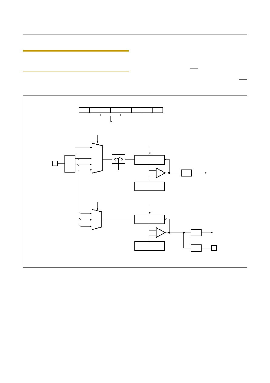
GMS82512/16/24
HYUNDAI MicroElectronics
36
FEB. 2000 Ver 1.00
Note: The contents of Timer data register TDRx should be
initialized 1
H
~FF
H
, not 0
H
, because it is undefined after re-
set.
In the Timer 0, timer register T0 increments from 00
H
until
it matches TDR0 and then reset to 00H. The match output
of Timer 0 generates Timer 0 interrupt (latched in T0IF bit)
As TDRx and Tx register are in same address, when read-
ing it as a Tx, written to TDRx.
In counter function, the counter is increased every 1-to-0
(falling edge) transition of EC0 pin. In order to use counter
function, the bit 4 of the Port mode register PMR4 are set
to "1". The Timer 0 can be used as a counter by pin EC0
input, but Timer 1 can input by internal clock.
Figure 11-3 8-bit Timer/Counter 2, 3
Example 3:
Timer2 = 8-bit timer mode, 2ms interval at 8MHz
Timer3 = 8-bit timer mode, 500us interval at 8MHz
LDM
TDR2,#250
LDM
TDR3,#250
LDM
TM2,#0110_1111B
SET1
T2E
SET1
T3E
EI
Example 4:
Timer2 = 8-bit event counter mode
Timer3 = 500us 8-bit timer mode at 8MHz
LDM
TDR2,#250
LDM
TDR3,#250
LDM
TM2,#0110_1100B
SET1
T2E
SET1
T3E
EI
÷
4
÷
16
÷
64
XIN PIN
MUX
Prescal
e
r
T2IF
clear
0: Stop
1: Clear and start
T2ST
T2SL[1:0]
00
01
10
11
TIMER 2
INTERRUPT
T2CN
MUX
T3IF
clear
0: Stop
1: Clear and start
T3ST
T3SL[1:0]
01
10
11
TIMER 3
INTERRUPT
÷
4
÷
16
÷
64
TDR2 (8-bit)
TDR3 (8-bit)
T3 (8-bit)
T2 (8-bit)
Comparator
Comparator
TIMER 2
TIMER 3
T3O PIN
F/F
BTCL
7
6
5
4
3
2
1
0
T3ST
CAP2
T2SL1
INITIAL VALUE: 00
H
ADDRESS: 0E3
H
TM2
T2SL0
T2CN
T2ST
T3SL1 T3SL0
0
X
X
X
X
X
X means don't care
01 or 10 or 11
Reserved
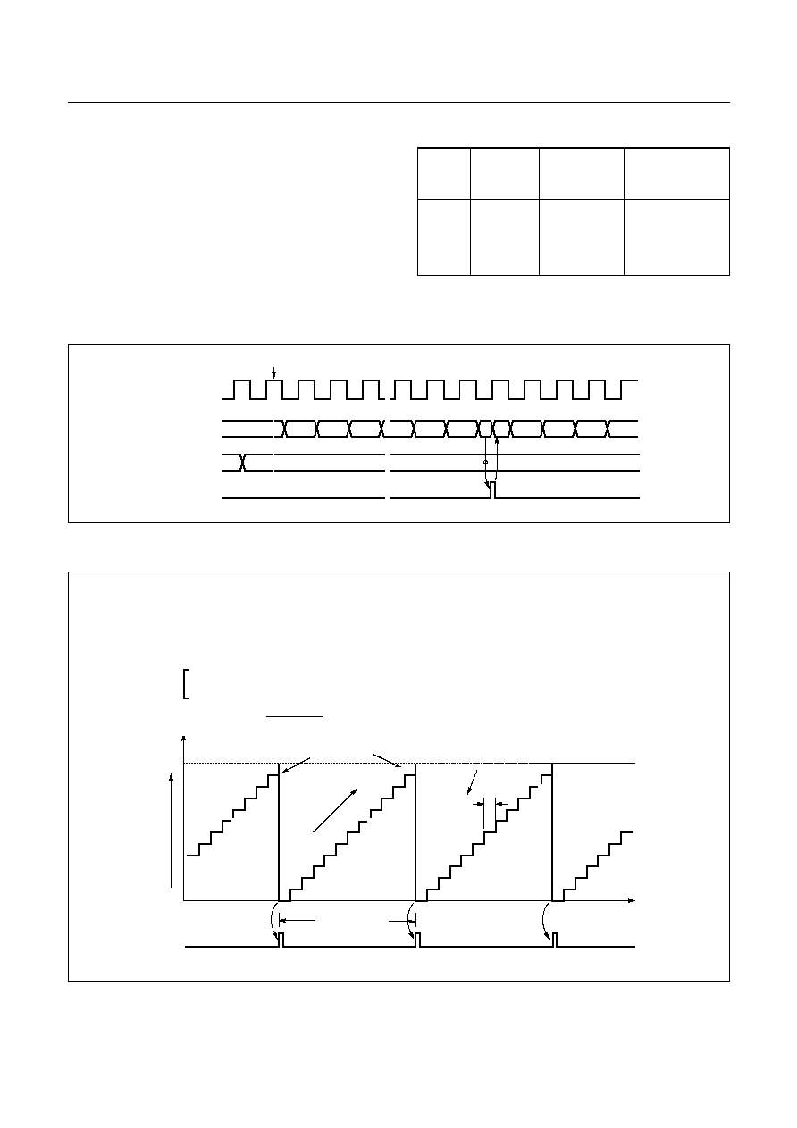
HYUNDAI MicroElectronics
GMS82512/16/24
FEB. 2000 Ver 1.00
37
8-bit Timer Mode
In the timer mode, the internal clock is used for counting
up. Thus, you can think of it as counting internal clock in-
put. The contents of TDRn are compared with the contents
of up-counter, Tn. If match is found, a timer 1 interrupt
(T1IF) is generated and the up-counter is cleared to 0.
Counting up is resumed after the up-counter is cleared.
As the value of TDRn is changeable by software, time in-
terval is set as you want
Figure 11-4 Timer Mode Timing Chart
Figure 11-5 Timer Count Example
Value of
TM[1:0]
Clock
Source
Resolution
(At f
XIN
=8 M H z)
Maximum Time
Setting
(At f
XIN
=8 M H z)
00
01
10
11
f
EC1
f
XIN
÷
4
f
XIN
÷
16
f
XIN
÷
64
1/f
EC1
0.5
2
8
sec
us
us
us
1/f
EC1
×
256
128
512
2048
sec
us
us
us
Table 11-1 Timer Source clock Interrupt Time
0
n-2
2
0
n
3
n-1
n
Source clock
Up-counter
TDR1
T1IF interrupt
Start count
1
2
3
1
4
Match
Detect
Counter
Clear
~~
~~
~~
~~
~~
~~
Timer 1 (T1IF)
Interrupt
TDR1
TIME
Occur interrupt
Occur interrupt
Occur interrupt
Interrupt period
up
-c
ou
nt
~~
~~
0
1
2
3
4
5
6
7A
7D
7C
Count Pulse
= 8
µ
s x 125
7B
MATCH
Example: Make 1ms
interrupt using by Timer0 at 8MHz
LDM
TM0,#1FH
; divide by 64
LDM
TDR0,#125
; 8us x 125= 1ms
SET1
T0E
; Enable Timer 0 Interrupt
EI
; Enable Master Interrupt
Period
When
TDR0 = 125
D
= 7D
H
f
XIN
= 8 MHz
INTERRUPT PERIOD =
8
×
106 Hz
1
×
64
×
125 = 1 ms
TM0 = 0001 1111
B
(8-bit Timer mode, Prescaler divide ratio = 64)
8
µ
s
(TDR0 = T0)
7D
0
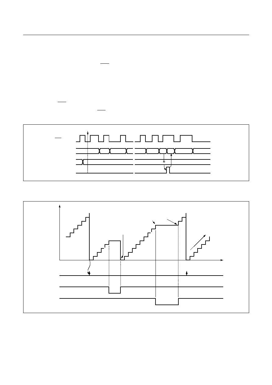
GMS82512/16/24
HYUNDAI MicroElectronics
38
FEB. 2000 Ver 1.00
8-bit Event Counter Mode
In this mode, counting up is started by an external trigger.
This trigger means falling edge of the EC0 pin input.
Source clock is used as an internal clock selected with tim-
er mode register TM0. The contents of timer data register
TDRn (n = 0,1) are compared with the contents of the up-
counter Tn. If a match is found, an timer interrupt request
flag TnIF is generated, and the counter is cleared to "0".
The counter is restart and count up continuously by every
falling edge of the EC0 pin input.
The maximum frequency applied to the EC0 pin is f
XIN
/2
[Hz].
In order to use event counter function, the bit 4 of the Port
Mode Register PMR4(address 0D0
H
) is required to be set
to "1".
After reset, the value of timer data register TDRn is unde-
fined, it should be initialized to between 1
H
~FF
H
not to
"0"The interval period of Timer is calculated as below
equation.
Figure 11-6 Event Counter Mode Timing Chart
Figure 11-7 Count Operation of Timer / Event counter
Period (sec)
1
f
XIN
-----------
2
Divide Ratio
TDRn
×
×
×
=
0
1
2
1
0
n
2
~~
~~
~~
n-1
n
~~
~~
~~
EC0 pin input
Up-counter
TDR1
T1IF interrupt
Start count
Timer 1 (T1IF)
Interrupt
TDR1
TIME
Occur interrupt
Occur interrupt
stop
clear & start
disable
enable
Start & Stop
T1ST
T1CN
Control count
up-
coun
t
~~
~~
T1ST = 0
T1ST = 1
T1CN = 0
T1CN = 1
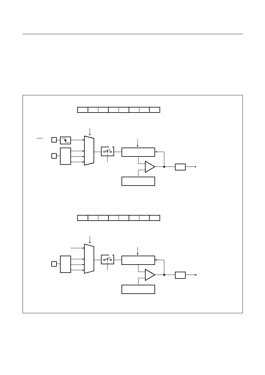
HYUNDAI MicroElectronics
GMS82512/16/24
FEB. 2000 Ver 1.00
39
11.2 16-bit Timer / Counter Mode
The Timer register is being run with all 16 bits. A 16-bit
timer/counter register T0, T1 are incremented from 0000
H
until it matches TDR0, TDR1 and then resets to 0000
H
.
The match output generates Timer 0 interrupt.
The clock source of the Timer 0 is selected either internal
or external clock by bit T0SL1, T0SL0.
Even if the Timer 0 (including the Timer 1) is used as a 16-
bit timer, the Timer 2 and Timer 3 can still be used as either
two 8-bit timer or one 16-bit timer by setting the TM2. Re-
versely, even if the Timer 2 (including the Timer 3) is used
as a 16-bit timer, the Timer 0 and Timer 1 can still be used
as 8-bit timer independently.
Figure 11-8 16-bit Timer/Counter
EC0 PIN
÷
4
÷
16
÷
64
XIN PIN
MUX
P
r
escal
e
r
T0IF
clear
0: Stop
1: Clear and start
T0ST
T0SL[1:0]
"00"
"01"
"10"
"11"
TIMER 0
INTERRUPT
T0CN
TDR1 + TDR0
Comparator
TIMER 0 + TIMER 1
TIMER 0 (16-bit)
Higher byte Lower byte
(16-bit)
COMPARE DATA
T1 + T0
(16-bit)
1
0
(Not Timer 1 interrupt)
EDGE DETECTOR
BTCL
7
6
5
4
3
2
1
0
T1ST
CAP0
T0SL1
INITIAL VALUE: 00
H
ADDRESS: 0E2
H
TM0
T0SL0
T0CN
T0ST
T1SL1 T1SL0
0
X
X
X
X
X
0
0
X means don't care
÷
4
÷
16
÷
64
XIN PIN
MUX
Pr
e
s
ca
le
r
T2IF
clear
0: Stop
1: Clear and start
T2ST
T2SL[1:0]
"00"
"01"
"10"
"11"
TIMER 2
INTERRUPT
T2CN
TDR3 + TDR2
Comparator
TIMER 2 + TIMER 3
TIMER 2 (16-bit)
Higher byte Lower byte
(16-bit)
COMPARE DATA
T3 + T2
(16-bit)
1
0
(Not Timer 3 interrupt)
Reserved
BTCL
7
6
5
4
3
2
1
0
T3ST
CAP2
T2SL1
INITIAL VALUE: 00
H
ADDRESS: 0E3
H
TM2
T2SL0
T2CN
T2ST
T3SL1 T3SL0
0
X
X
X
X
X
0
0
X means don't care
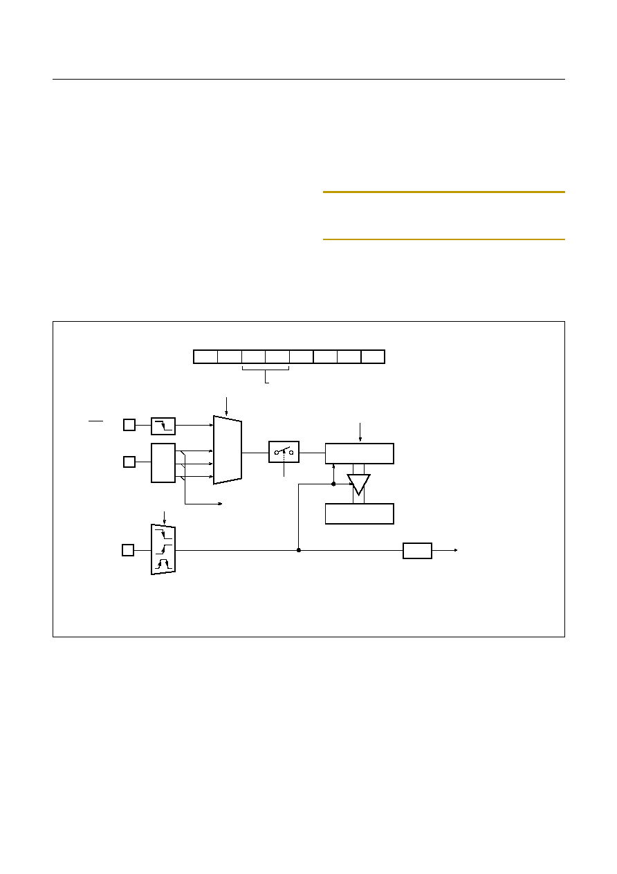
GMS82512/16/24
HYUNDAI MicroElectronics
40
FEB. 2000 Ver 1.00
11.3 8-bit Capture Mode
The Timer 0 capture mode is set by bit CAP0 of timer
mode register TM0 (bit CAP2 of timer mode register TM2
for Timer 2) as shown in Figure 21. In this mode, Timer 1
still operates as an 8-bit timer/counter.
As mentioned above, not only Timer 0 but Timer 2 can also
be used as a capture mode.
In 8-bit capture mode, Timer 1 and Timer 3 are can not be
used as a capture mode.
The Timer/Counter register is incremented in response in-
ternal or external input. This counting function is same
with normal timer mode, but Timer interrupt is not gener-
ated. Timer/Counter still does the above, but with the add-
ed feature that a edge transition at external input INTn pin
causes the current value in the Timer counter register
(T0,T2), to be captured into registers CDRn (CDR0,
CDR2), respectively. After captured, Timer counter regis-
ter is cleared and restarts by hardware.
Note: The CDRn and TDRn are in same address.In the
capture mode, reading operation is read the CDRn, not
TDRn because path is opened to the CDRn.
It has three transition modes: "falling edge", "rising edge",
"both edge" which are selected by interrupt edge selection
register IEDS. Refer to "14.4 External Interrupt" on page
51. In addition, the transition at INTn pin generate an inter-
rupt.
Figure 11-9 8-bit Capture Mode
EC0 PIN
÷
4
÷
16
÷
64
XIN PIN
MUX
Pr
e
s
ca
le
r
INT0IF
0: Stop
1: Clear and start
T0ST
T0SL[1:0]
"00"
"01"
"10"
"11"
INT0
INTERRUPT
T0CN
CDR0 (8-bit)
T0 (8-bit)
TIMER 0
BTCL
7
6
5
4
3
2
1
0
T1ST
CAP0
T0SL1
INITIAL VALUE: 00
H
ADDRESS: 0E2
H
TM0
T0SL0
T0CN
T0ST
T1SL1 T1SL0
1
X
X
X
X
X
X means don't care
01 or 10 or 11
"01"
"10"
"11"
INT0 PIN
Capture
To TIMER1
IEDS[1:0]
Edge Detector
This figure is a example of using the Timer0.
In the Timer2, operation is same like Timer0, each registers and
flags may be changed with for Timer2.
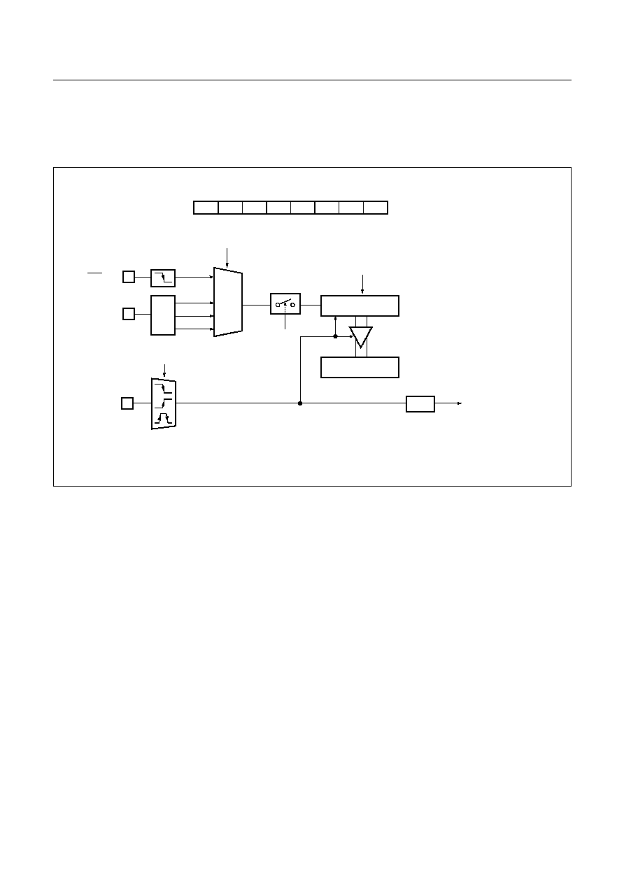
HYUNDAI MicroElectronics
GMS82512/16/24
FEB. 2000 Ver 1.00
41
11.4 16-bit Capture Mode
16-bit capture mode is the same as 8-bit capture, except
that the Timer register is being run will 16 bits.
Figure 11-10 16-bit Capture Mode
EC0 PIN
÷
4
÷
16
÷
64
XIN PIN
MUX
Prescal
e
r
INT0IF
0: Stop
1: Clear and start
T0ST
T0SL[1:0]
"00"
"01"
"10"
"11"
INT0
INTERRUPT
T0CN
BTCL
7
6
5
4
3
2
1
0
T1ST
CAP0
T0SL1
INITIAL VALUE: 00
H
ADDRESS: 0E2
H
TM0
T0SL0
T0CN
T0ST
T1SL1 T1SL0
1
X
X
X
X
X
X means don't care
"01"
"10"
"11"
INT0 PIN
Capture
IEDS[1:0]
Edge Detector
This figure is a example of using the Timer0, 1.
In the Timer2, 3, operation is same like Timer0,1, each registers and
flags may be changed with for Timer2,3.
CDR1 + CDR0
Higher byte Lower byte
(16-bit)
CAPTURE DATA
T1 + T0
(16-bit)
0
0
TIMER 0 + TIMER 1
TIMER 0 (16-bit)

GMS82512/16/24
HYUNDAI MicroElectronics
42
FEB. 2000 Ver 1.00
Example 1:
Timer0 = 16-bit timer mode, 0.5s at 8MHz
Timer2 = 2ms 8-bit timer mode at 8MHz
Timer3 = 250us 8-bit timer mode at 8MHz
LDM
TDR0,#23H
LDM
TDR1,#0F4H
LDM
TM0,#0FH
LDM
TDR2,#249
LDM
TDR3,#124
LDM
TM2,#0110_1111B
SET1
T0E
SET1
T2E
SET1
T3E
EI
:
:
Example 2:
Timer0 = 8-bit timer mode, 2ms interval at 8MHz
Timer2 = 16-bit event counter mode
LDM
TDR0,#249
LDM
TM0,#0111_1111B
LDM
TDR2,#3FH
LDM
TDR3,#2AH
LDM
TM2,#0100_1100B
SET1
T0E
SET1
T2E
EI
:
:
Example 3:
Timer0 = 8-bit timer mode, 2ms interval at 8MHz
Timer2 = 8-bit capture mode
LDM
TDR0,#250
LDM
TM0,#0111_1111B
SET1
T0E
LDM
TDR2,#40H
LDM
TDR3,#2AH
LDM
TM2,#1111_1111B
SET1
T2E
LDM
IEDS,#XX11_XXXXB
LDM
PMR4,#XXXX_X1XXB
SET1
INT2E
EI
:
:
X: don't care.
Example 4:
Timer0 = 8-bit timer mode, 2ms interval at 8MHz
Timer2 = 16-bit capture mode
LDM
TDR0,#249
LDM
TM0,#0111_1111B
SET1
T0E
LDM
TDR2,#40H
LDM
TDR3,#2AH
LDM
TM2,#1100_1111B
SET1
T2E
LDM
IEDS,#XX11_XXXXB
LDM
PMR4,#XXXX_X1XXB
SET1
INT2E
EI
:
:
X: don't care.
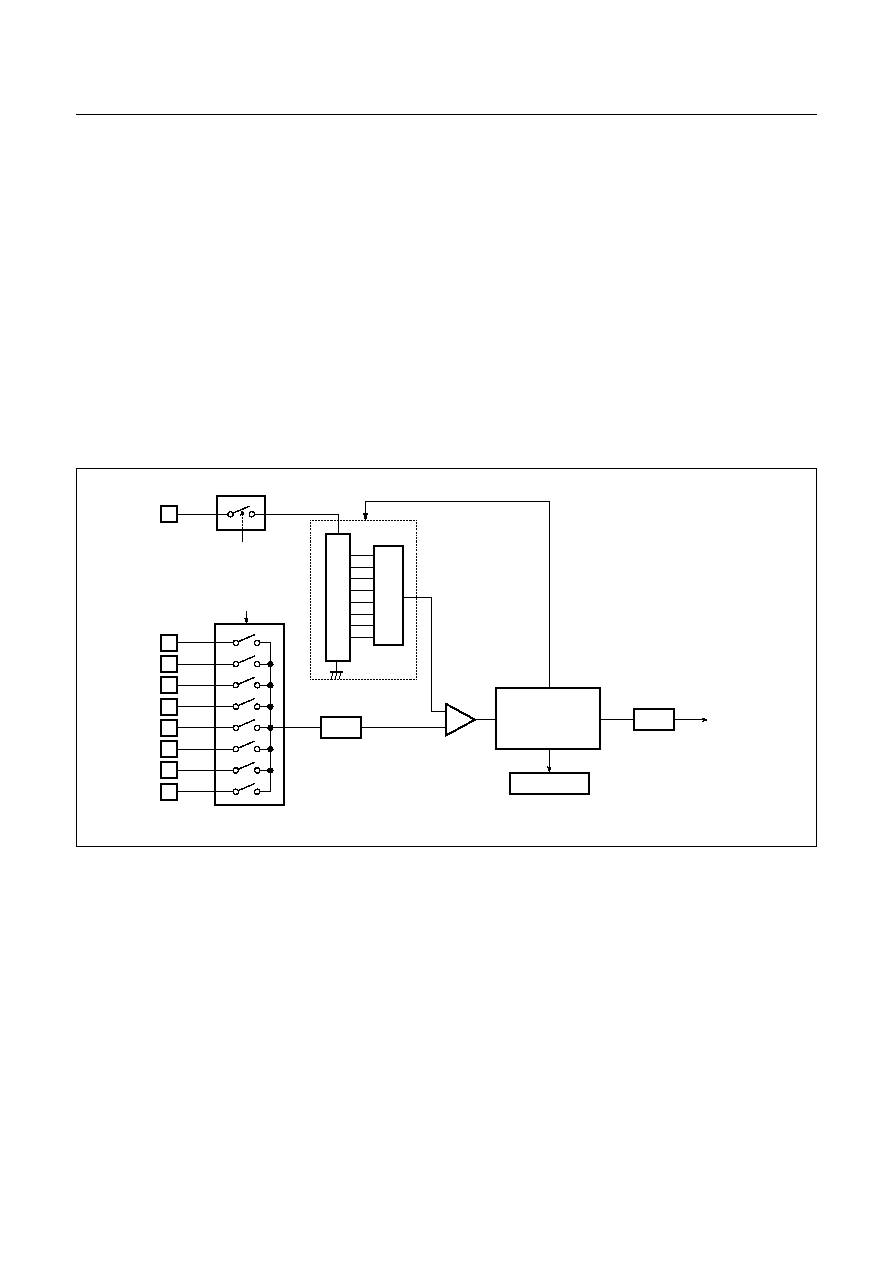
HYUNDAI MicroElectronics
GMS82512/16/24
FEB. 2000 Ver 1.00
43
12. ANALOG DIGITAL CONVERTER
The analog-to-digital converter (A/D) allows conversion
of an analog input signal to a corresponding 8-bit digital
value. The A/D module has eight analog inputs, which are
multiplexed into one sample and hold. The output of the
sample and hold is the input into the converter, which gen-
erates the result via successive approximation. The analog
supply voltage is connected to AV
DD
of ladder resistance
of A/D module.
The A/D module has two registers which are the control
register ADCM and A/D result register ADR. The register
ADCM, shown in Figure 12-2, controls the operation of
the A/D converter module. The port pins can be configured
as analog inputs or digital I/O. To use analog inputs, I/O is
selected input mode by R3DD or R6DD direction register.
How to Use A/D Converter
The processing of conversion is start when the start bit
ADST is set to "1". After one cycle, it is cleared by hard-
ware. The register ADR contains the results of the A/D
conversion. When the conversion is completed, the result
is loaded into the ADR, the A/D conversion status bit
ADSF is set to "1", and the A/D interrupt flag AIF is set.
The block diagram of the A/D module is shown in Figure
12-1. The A/D status bit ADSF is set automatically when
A/D conversion is completed, cleared when A/D conver-
sion is in process. The conversion time takes maximum 20
uS (at f
XIN
=8 MHz).
Figure 12-1 A/D Block Diagram
R30/AN0
R31/AN1
R32/AN2
R33/AN3
R64/AN4
R65/AN5
R66/AN6
R67/AN7
S/H
Sample & Hold
"0"
"1"
ADEN
AV
DD
8-bit
DA
C
L
A
DDER RESIS
TO
R
ADIF
A/D
INTERRUPT
SUCCESSIVE
APPROXIMATION
CIRCUIT
ADR
A/D result register
ADDRESS: E9
H
RESET VALUE: Undefined
000
001
010
011
100
101
110
111
ADS[2:0]
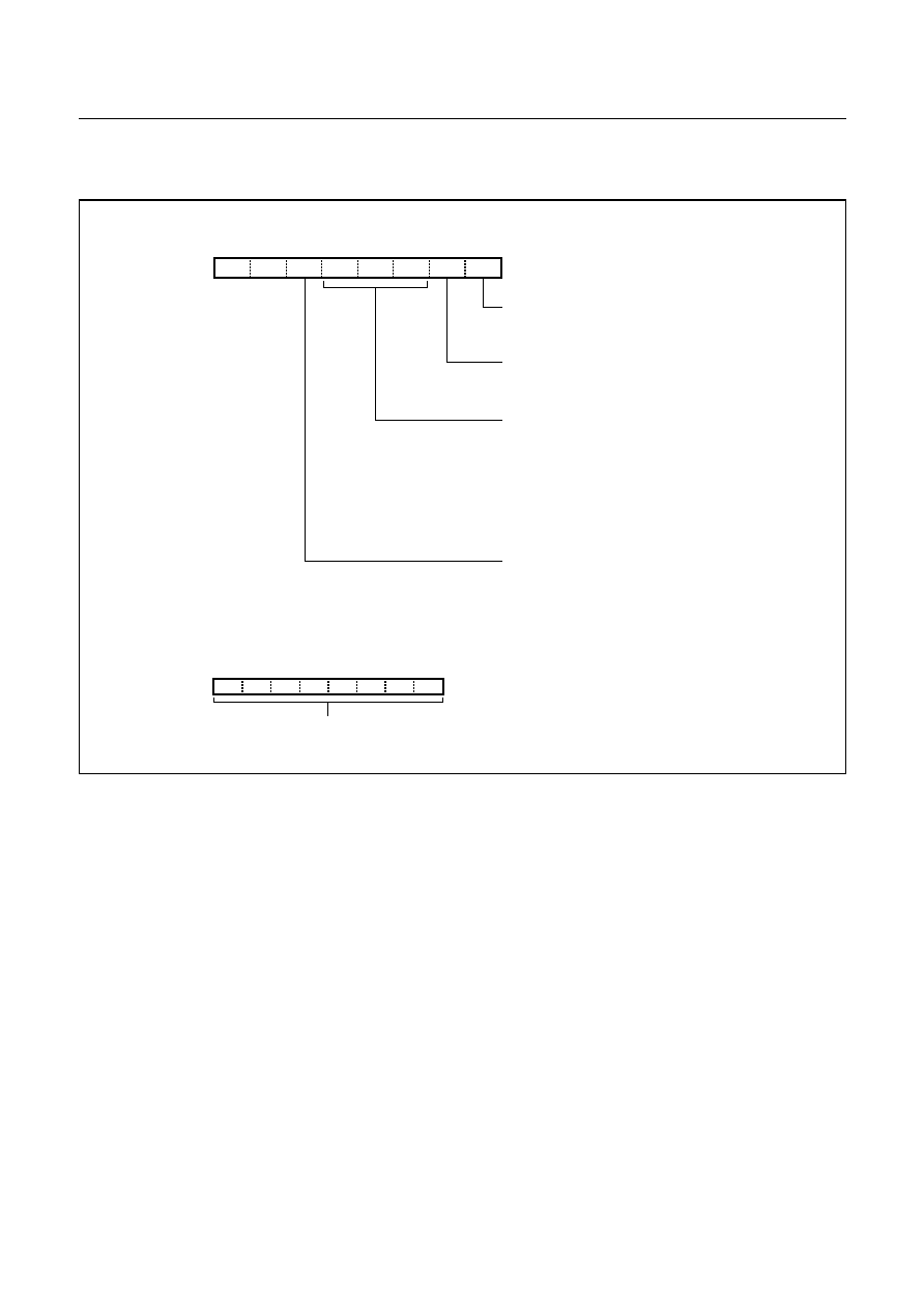
GMS82512/16/24
HYUNDAI MicroElectronics
44
FEB. 2000 Ver 1.00
Figure 12-2 A/D Converter Control Register
BTCL
7
6
5
4
3
2
1
0
-
-
ADST
A/D status bit
Analog input channel select
INITIAL VALUE: --00 0001
B
ADDRESS: 0E8
H
ADCM
ADSF
A/D converter Enable bit
0: A/D converter module turn off and
current is not flow.
1: Enable A/D converter
R/W
R/W
R/W
R/W
R/W
R
000: Channel 0 (AN0)
001: Channel 1 (AN1)
010: Channel 2 (AN2)
011: Channel 3 (AN3)
100: Channel 4 (AN4)
101: Channel 5 (AN5)
110: Channel 6 (AN6)
111: Channel 7 (AN7)
0: A/D conversion is in progress
1: A/D conversion is completed
A/D start bit
Setting this bit starts an A/D conversion.
After one cycle, bit is cleared to "0" by hardware.
ADS1 ADS0
ADEN ADS2
INITIAL VALUE: Undefined
ADDRESS: 0E9
H
ADR
A/D Conversion Data
BTCL
7
6
5
4
3
2
1
0
R
R
R
R
R
R
R
R
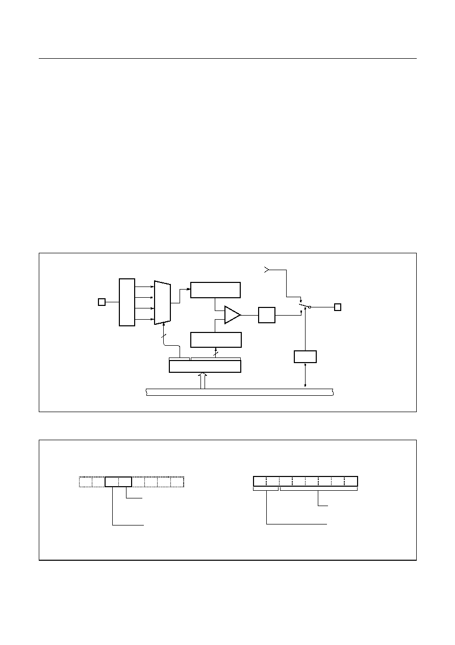
HYUNDAI MicroElectronics
GMS82512/16/24
FEB. 2000 Ver 1.00
45
13. BUZZER FUNCTION
The buzzer driver block consists of 6-bit binary counter,
buzzer register, and clock source selector. It generates
square-wave which has very wide range frequency (500Hz
~ 250kHz at f
XIN
= 8MHz) by user software.
A 50% duty pulse can be output to R55/BUZ pin to use for
piezo-electric buzzer drive
. Pin R55 is assigned for output port
of Buzzer driver by setting the bit 5 of PMR5 (address D1
H
) to
"1".
At this time, the pin R55 must be defined as output
mode (the bit 5 of R5DD=1).
Example: 2.4kHz output at 8MHz.
LDM
R5DD,#XX1X_XXXXB
LDM
BUR,#9AH
LDM
PMR5,#XX1X_XXXXB
X means don't care
The bit 0 to 5 of BUR determines output frequency for
buzzer driving.
Equation of frequency calculation is shown below.
f
BUZ
: Buzzer frequency
f
XIN
: Oscillator frequency
Divide Ratio: Prescaler divide ratio by BUCK[1:0]
BUR: Lower 6-bit value of BUR. Buzzer period value.
The frequency of output signal is controlled by the buzzer
control register BUR.The bit 0 to bit 5 of BUR determine
output frequency for buzzer driving.
Figure 13-1 Block Diagram of Buzzer Driver
Figure 13-2 PMR5 and Buzzer Register
f
B UZ
f
XIN
2
DivideRatio
B UR
×
×
-------------------------------------------------------------
=
P
r
escal
e
r
÷
16
÷
64
÷
32
÷
128
BUR
R55/BUZ PIN
PMR5
Internal bus line
R55 port data
XIN PIN
6-bit binary
2
6
[0EC
H
]
[0D1
H
]
0
1
F/F
÷
2
Comparator
Compare data
6-BIT COUNTER
MUX
00
01
10
11
Port selection
BUR[5:0]
BUR
ADDRESS: 0EC
H
RESET VALUE: Undefined
W
W
W
W
W
W
Source clock select
00:
÷
16
01:
÷
32
10:
÷
64
11:
÷
128
Buzzer Period Data
R55/BUZ Selection
PMR5
ADDRESS: 0D1
H
RESET VALUE: --00 ----
B
W
-
-
0: R55 port (Turn off buzzer)
1: BUZ port (Turn on buzzer)
W
W
-
-
-
-
W
R54/WDTO Selection
0: R54
1: WDTO (Output)
BUCK1 BUCK0

GMS82512/16/24
HYUNDAI MicroElectronics
46
FEB. 2000 Ver 1.00
Note: BUR is undefined after reset, so it must be initialized
to between 1
H
and 3F
H
by software.
Note that BUR is a write-only register.
The 6-bit counter is cleared and starts the counting by writ-
ing signal at BUR register. It is incremental from 00
H
until
it matches 6-bit BUR value.
When main-frequency is 8MHz, buzzer frequency is
shown as below table.
[kHz]
BUR
[5:0]
BUR[7:6]
BUR
[5:0]
BUR[7:6]
00
01
10
11
00
01
10
11
00
01
02
03
04
05
06
07
-
250.000
125.000
83.333
62.500
50.000
41.667
35.714
-
125.000
62.500
41.667
31.250
25.000
20.833
17.857
-
62.500
31.250
20.833
15.625
12.500
10.417
8.929
-
31.250
15.625
10.417
7.813
6.250
5.208
4.464
20
21
22
23
24
25
26
27
7.813
7.576
7.353
7.143
6.944
6.757
6.579
6.410
3.906
3.788
3.676
3.571
3.472
3.378
3.289
3.205
1.953
1.894
1.838
1.786
1.736
1.689
1.645
1.603
0.977
0.947
0.919
0.893
0.868
0.845
0.822
0.801
08
09
0A
0B
0C
0D
0E
0F
31.250
27.778
25.000
22.727
20.833
19.231
17.857
16.667
15.625
13.889
12.500
11.364
10.417
9.615
8.929
8.333
7.813
6.944
6.250
5.682
5.208
4.808
4.464
4.167
3.906
3.472
3.125
2.841
2.604
2.404
2.232
2.083
28
29
2A
2B
2C
2D
2E
2F
6.250
6.098
5.952
5.814
5.682
5.556
5.435
5.319
3.125
3.049
2.976
2.907
2.841
2.778
2.717
2.660
1.563
1.524
1.488
1.453
1.420
1.389
1.359
1.330
0.781
0.762
0.744
0.727
0.710
0.694
0.679
0.665
10
11
12
13
14
15
16
17
15.625
14.706
13.889
13.158
12.500
11.905
11.364
10.870
7.813
7.353
6.944
6.579
6.250
5.952
5.682
5.435
3.906
3.676
3.472
3.289
3.125
2.976
2.841
2.717
1.953
1.838
1.736
1.645
1.563
1.488
1.420
1.359
30
31
32
33
34
35
36
37
5.208
5.102
5.000
4.902
4.808
4.717
4.630
4.545
2.604
2.551
2.500
2.451
2.404
2.358
2.315
2.273
1.302
1.276
1.250
1.225
1.202
1.179
1.157
1.136
0.651
0.638
0.625
0.613
0.601
0.590
0.579
0.568
18
19
1A
1B
1C
1D
1E
1F
10.417
10.000
9.615
9.259
8.929
8.621
8.333
8.065
5.208
5.000
4.808
4.630
4.464
4.310
4.167
4.032
2.604
2.500
2.404
2.315
2.232
2.155
2.083
2.016
1.302
1.250
1.202
1.157
1.116
1.078
1.042
1.008
38
39
3A
3B
3C
3D
3E
3F
4.464
4.386
4.310
4.237
4.167
4.098
4.032
3.968
2.232
2.193
2.155
2.119
2.083
2.049
2.016
1.984
1.116
1.096
1.078
1.059
1.042
1.025
1.008
0.992
0.558
0.548
0.539
0.530
0.521
0.512
0.504
0.496
Table 13-1 Buzzer Frequency
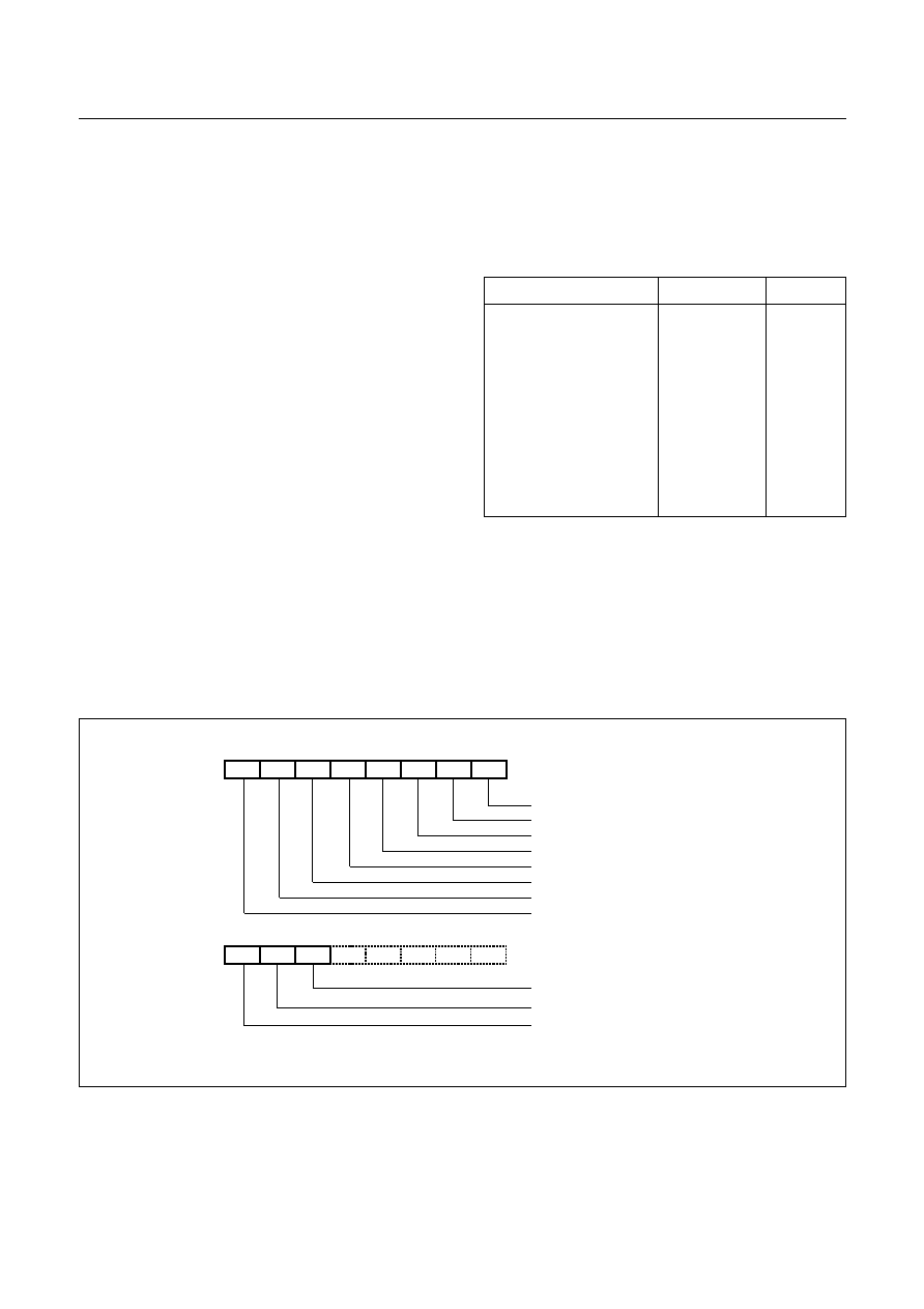
HYUNDAI MicroElectronics
GMS82512/16/24
FEB. 2000 Ver 1.00
47
14. INTERRUPTS
The GMS825xx interrupt circuits consist of Interrupt en-
able register (IENH, IENL), Interrupt request flags of
IRQH, IRQL, Priority circuit, and Master enable flag ("I"
flag of PSW). Thirteen interrupt sources are provided. The
configuration of interrupt circuit is shown in Figure 14-2.
The External Interrupts INT0 ~ INT3 each can be transi-
tion-activated (1-to-0 or 0-to-1 transition) by selection
IEDS.
The flags that actually generate these interrupts are bit
INT0F, INT1F, INT2F and INT3F in register IRQH. When
an external interrupt is generated, the flag that generated it
is cleared by the hardware when the service routine is vec-
tored to only if the interrupt was transition-activated.
The Timer 0 ~ Timer 3 Interrupts are generated by TxIF
which is set by a match in their respective timer/counter
register. The Basic Interval Timer Interrupt is generated by
BITIF which is set by an overflow in the timer register.
The AD converter Interrupt is generated by ADIF which is
set by finishing the analog to digital conversion.
The Watchdog timer Interrupt is generated by WDTIF
which set by a match in Watchdog timer register.
The Basic Interval Timer Interrupt is generated by BITIF
which are set by a overflow in the timer counter register.
The interrupts are controlled by the interrupt master enable
flag I-flag (bit 2 of PSW on page 16), the interrupt enable
register (IENH, IENL), and the interrupt request flags (in
IRQH and IRQL) except Power-on reset and software
BRK interrupt. Below table shows the Interrupt priority.
Vector addresses are shown in Figure 8-6 on page 18. In-
terrupt enable registers are shown in Figure 14-3. These
registers are composed of interrupt enable flags of each in-
terrupt source and these flags determines whether an inter-
rupt will be accepted or not. When enable flag is "0", a
corresponding interrupt source is prohibited. Note that
PSW contains also a master enable bit, I-flag, which dis-
ables all interrupts at once.
Figure 14-1 Interrupt Request Flag
Reset/Interrupt
Symbol
Priority
Hardware Reset
External Interrupt 0
External Interrupt 1
External Interrupt 2
External Interrupt 3
Timer/Counter 0
Timer/Counter 1
Timer/Counter 2
Timer/Counter 3
ADC Interrupt
Basic Interval Timer
Watchdog Timer
RESET
INT0
INT1
INT2
INT3
Timer 0
Timer 1
Timer 2
Timer 3
ADC
BIT
WDT
1
2
3
4
5
6
7
8
9
10
11
12
INT3IF
R/W
INT0IF
Timer/Counter 3 interrupt request flag
INITIAL VALUE: 0000 0000
B
ADDRESS: 0F7
H
IRQH
INT1IF
MSB
LSB
T2IF
T3IF
T0IF
T1IF
INT2IF
R/W
R/W
Timer/Counter 2 interrupt request flag
Timer/Counter 1 interrupt request flag
External interrupt 3 request flag
R/W
ADIF
INITIAL VALUE: 000- ----
B
ADDRESS: 0F5
H
IRQL
WDTIF
MSB
LSB
-
-
-
BITIF
Timer/Counter 0 interrupt request flag
R/W
R/W
-
R/W
R/W
R/W
R/W
R/W
Basic Interval Timer interrupt request flag
Watchdog timer interrupt request flag
A/D Converter interrupt request flag
External interrupt 3 request flag
External interrupt 3 request flag
External interrupt 3 request flag
-
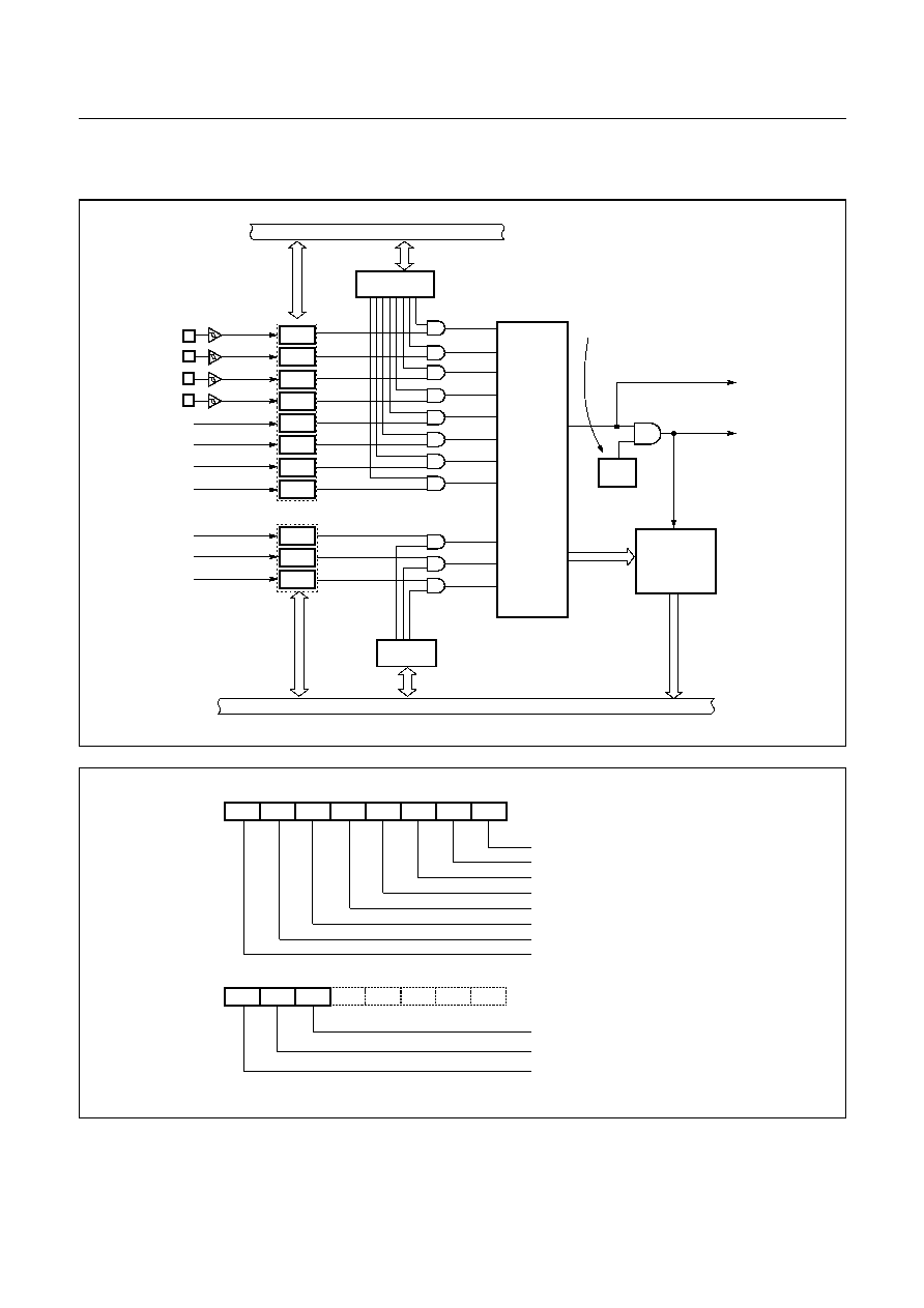
GMS82512/16/24
HYUNDAI MicroElectronics
48
FEB. 2000 Ver 1.00
.
Figure 14-2 Block Diagram of Interrupt
Figure 14-3 Interrupt Enable Flag
Timer 0
INT2
INT1
INT0
INT0IF
IENH
Interrupt Enable
Interrupt Enable
IRQH
IRQL
Interrupt
Vector
Address
Generator
Internal bus line
Register (Lower byte)
Internal bus line
Register (Higher byte)
Release STOP
To CPU
Interrupt Master
Enable Flag
I-flag
IENL
P
r
i
o
ri
t
y
Control
I-flag is in PSW, it is cleared by "DI", set by
"EI" instruction. When it goes interrupt service,
I-flag is cleared by hardware, thus any other
interrupt are inhibited. When interrupt service is
completed by "RETI" instruction, I-flag is set to
"1" by hardware.
[0F6
H
]
[0F4
H
]
[0F7
H
]
[0F5
H
]
INT1IF
INT2IF
INT3IF
T0IF
T3IF
T2IF
INT3
Timer 1
Timer 3
Timer 2
T1IF
A/D Converter
ADIF
BITIF
Watchdog Timer
BIT
WDTIF
INT3E
R/W
INT0E
Timer/Counter 3 interrupt enable flag
INITIAL VALUE: 0000 0000
B
ADDRESS: 0F6
H
IENH
INT1E
MSB
LSB
T2E
T3E
T0E
T1E
INT2E
R/W
R/W
Timer/Counter 2 interrupt enable flag
Timer/Counter 1 interrupt enable flag
External interrupt 3 enable flag
R/W
ADE
INITIAL VALUE: 000- ----
B
ADDRESS: 0F4
H
IENL
WDTE
MSB
LSB
-
-
-
BITE
Timer/Counter 0 interrupt enable flag
R/W
R/W
-
R/W
R/W
R/W
R/W
R/W
Basic Interval Timer interrupt enable flag
Watchdog timer interrupt enable flag
A/D Converter interrupt enable flag
External interrupt 2 enable flag
External interrupt 1 enable flag
External interrupt 0 enable flag
0: Disable
1: Enable
VALUE
-
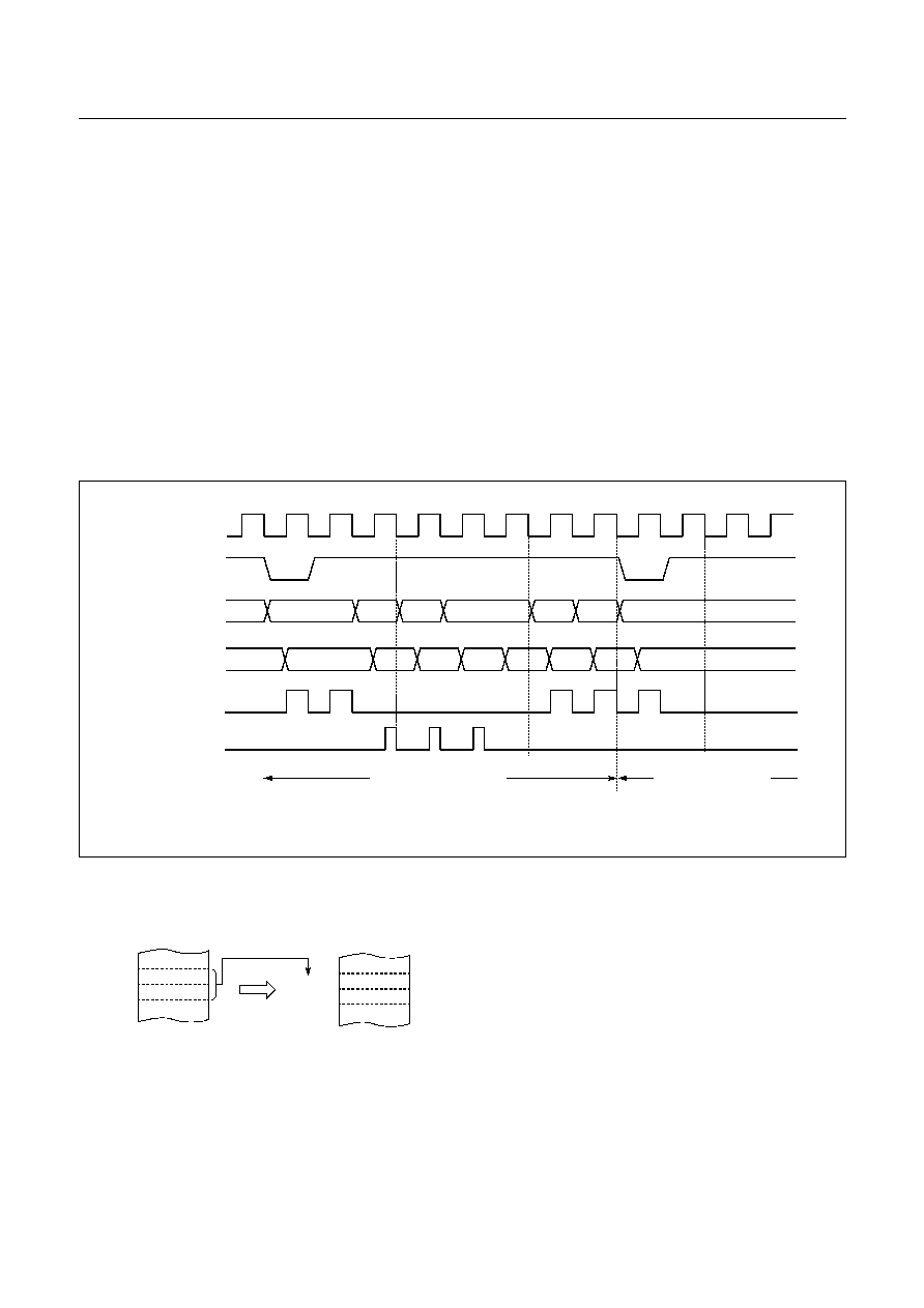
HYUNDAI MicroElectronics
GMS82512/16/24
FEB. 2000 Ver 1.00
49
14.1 Interrupt Sequence
An interrupt request is held until the interrupt is accepted
or the interrupt latch is cleared to "0" by a reset or an in-
struction. Interrupt acceptance sequence requires 8
f
XIN
(2
µ
s at f
MAIN
=4.19MHz) after the completion of the current
instruction execution. The interrupt service task is termi-
nated upon execution of an interrupt return instruction
[RETI].
Interrupt acceptance
1. The interrupt master enable flag (I-flag) is cleared to
"0" to temporarily disable the acceptance of any follow-
ing maskable interrupts. When a non-maskable inter-
rupt is accepted, the acceptance of any following
interrupts is temporarily disabled.
2. Interrupt request flag for the interrupt source accepted is
cleared to "0".
3. The contents of the program counter (return address)
and the program status word are saved (pushed) onto the
stack area. The stack pointer decreases 3 times.
4. The entry address of the interrupt service program is
read from the vector table address and the entry address
is loaded to the program counter.
5. The instruction stored at the entry address of the inter-
rupt service program is executed.
Figure 14-4 Timing chart of Interrupt Acceptance and Interrupt Return Instruction
A interrupt request is not accepted until the I-flag is set to
"1" even if a requested interrupt has higher priority than
that of the current interrupt being serviced.
When nested interrupt service is required, the I-flag should
be set to "1" by "EI" instruction in the interrupt service
program. In this case, acceptable interrupt sources are se-
lectively enabled by the individual interrupt enable flags.
Saving/Restoring General-purpose Register
During interrupt acceptance processing, the program
counter and the program status word are automatically
saved on the stack, but accumulator and other registers are
not saved itself. These registers are saved by the software
if necessary. Also, when multiple interrupt services are
nested, it is necessary to avoid using the same data memory
V.L.
System clock
Address Bus
PC
SP
SP-1
SP-2
V.H.
New PC
V.L.
Data Bus
Not used
PCH
PCL
PSW
ADL
OP code
ADH
Instruction Fetch
Internal Read
Internal Write
Interrupt Processing Step
Interrupt Service Task
V.L. and V.H. are vector addresses.
ADL and ADH are start addresses of interrupt service routine as vector contents.
Basic Interval Timer
012
H
0E3
H
0FFE6
H
0FFE7
H
0E
H
2E
H
0E312
H
0E313
H
Entry Address
Correspondence between vector table address for BIT interrupt
and the entry address of the interrupt service program.
Vector Table Address
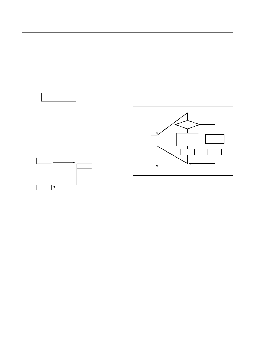
GMS82512/16/24
HYUNDAI MicroElectronics
50
FEB. 2000 Ver 1.00
area for saving registers.
The following method is used to save/restore the general-
purpose registers.
Example: Register save using push and pop instructions
General-purpose register save/restore using push and pop
instructions;
14.2 BRK Interrupt
Software interrupt can be invoked by BRK instruction,
which has the lowest priority order.
Interrupt vector address of BRK is shared with the vector
of TCALL 0 (Refer to Program Memory Section). When
BRK interrupt is generated, B-flag of PSW is set to distin-
guish BRK from TCALL 0.
Each processing step is determined by B-flag as shown in
Figure 14-5.
Figure 14-5 Execution of BRK/TCALL0
INTxx:
PUSH
A
PUSH
X
PUSH
Y
;SAVE ACC.
;SAVE X REG.
;SAVE Y REG.
interrupt processing
POP
Y
POP
X
POP
A
RETI
;RESTORE Y REG.
;RESTORE X REG.
;RESTORE ACC.
;RETURN
main task
interrupt
service task
saving
registers
restoring
registers
acceptance of
interrupt
interrupt return
B-FLAG
BRK
INTERRUPT
ROUTINE
RETI
TCALL0
ROUTINE
RET
BRK or
TCALL0
=0
=1
HYUNDAI MicroElectronics
GMS82512/16/24
FEB. 2000 Ver 1.00
51
14.3 Multi Interrupt
If two requests of different priority levels are received si-
multaneously, the request of higher priority level is ser-
viced. If requests of the interrupt are received at the same
time simultaneously, an internal polling sequence deter-
mines by hardware which request is serviced.
Figure 14-6 Execution of Multi Interrupt
However, multiple processing through software for special
features is possible. Generally when an interrupt is accept-
ed, the I-flag is cleared to disable any further interrupt. But
as user sets I-flag in interrupt routine, some further inter-
rupt can be serviced even if certain interrupt is in progress.
Example: During Timer1 interrupt is in progress, INT0 in-
terrupt serviced without any suspend.
TIMER1:
PUSH
A
PUSH
X
PUSH
Y
LDM
IENH,#80H
;
Enable INT0 only
LDM
IENL,#0
;
Disable other
EI
;
Enable Interrupt
:
:
:
:
:
:
LDM
IENH,#0FFH
;
Enable all interrupts
LDM
IENL,#0F0H
POP
Y
POP
X
POP
A
RETI
14.4 External Interrupt
The external interrupt on INT0, INT1, INT2 and INT3 pins
are edge triggered depending on the edge selection register
IEDS (address 0F8
H
) as shown in Figure 14-7.
The edge detection of external interrupt has three transition
enable INT0
TIMER 1
service
INT0
service
Main Program
service
Occur
TIMER1 interrupt
Occur
INT0
EI
disable other
enable INT0
enable other
In this example, the INT0 interrupt can be serviced without any
pending, even TIMER1 is in progress.
Because of re-setting the interrupt enable registers IENH,IENL
and master enable "EI" in the TIMER1 routine.
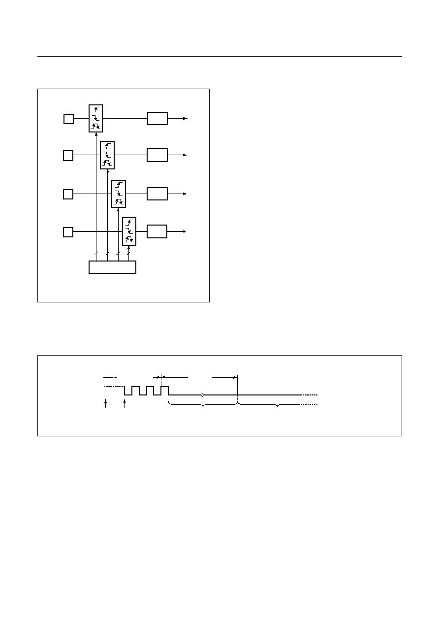
GMS82512/16/24
HYUNDAI MicroElectronics
52
FEB. 2000 Ver 1.00
activated mode: rising edge, falling edge, and both edge.
Figure 14-7 External Interrupt Block Diagram
INT0 ~ INT3 are multiplexed with general I/O ports
(R40~R43). To use as an external interrupt pin, the bit of
R4 port mode register PMR4 should be set to "1" corre-
spondingly.
Example: To use as an INT0 and INT2
:
:
;
**** Set port as an input port R40,R42
LDM
R4DD,#1111_1010B
;
;
**** Set port as an external interrupt port
LDM
PMR4,#05H
;
;
**** Set Falling-edge Detection
LDM
IEDS,#0001_0001B
:
:
:
Response Time
The INT0 ~ INT3 edge are latched into INT1IF ~ INT3IF
at every machine cycle. The values are not actually polled
by the circuitry until the next machine cycle. If a request is
active and conditions are right for it to be acknowledged, a
hardware subroutine call to the requested service routine
will be the next instruction to be executed. The DIV itself
takes twelve cycles. Thus, a minimum of twelve complete
machine cycles elapse between activation of an external
interrupt request and the beginning of execution of the first
instruction of the service routine.
Figure 14-8shows interrupt response timings.
Figure 14-8 Interrupt Response Timing Diagram
INT0IF
INT0 pin
INT0 INTERRUPT
INT1IF
INT1 pin
INT1 INTERRUPT
INT2IF
INT2 pin
INT2 INTERRUPT
IEDS
[0F8H]
INT3IF
INT3 pin
INT3 INTERRUPT
Edge selection
Register
2
2
2
2
Interrupt
goes
active
Interrupt
latched
Interrupt
processing
Interrupt
routine
8 f
XIN
max. 12 f
XIN
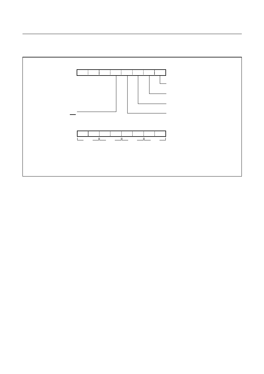
HYUNDAI MicroElectronics
GMS82512/16/24
FEB. 2000 Ver 1.00
53
Figure 14-9 PMR4 and IEDS Registers
BTCL
W
W
W
W
W
-
-
-
INT1S
0: R40
1: INT0
INITIAL VALUE: 00
H
ADDRESS: 0D0
H
PMR4
EC0S
INT0S
INT2S
INT3S
0: R41
1: INT1
0: R42
1: INT2
0: R43
1: INT3
0: R44
1: EC0
LSB
MSB
BTCL
W
W
W
W
W
W
W
W
IED2H
IED3L
IED3H
IED0H
INITIAL VALUE: 00
H
ADDRESS: 0F8
H
IEDS
IED2L
IED0L
IED1L
IED1H
LSB
MSB
Edge selection register
00: Reserved
01: Falling (1-to-0 transition)
10: Rising (0-to-1 transition)
11: Both (Rising & Falling)
INT0
INT1
INT2
INT3
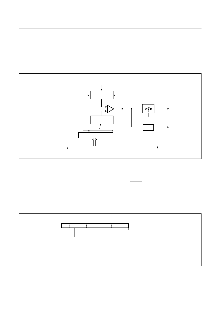
GMS82512/16/24
HYUNDAI MicroElectronics
54
FEB. 2000 Ver 1.00
15. WATCHDOG TIMER
The watchdog timer rapidly detects the CPU malfunction
such as endless looping caused by noise or the like, and re-
sumes the CPU to the normal state.
The watchdog timer signal for detecting malfunction can
be selected either a reset CPU or a interrupt request.
When the watchdog timer is not being used for malfunc-
tion detection, it can be used as a timer to generate an in-
terrupt at fixed intervals.
Figure 15-1 Block Diagram of Watchdog Timer
Watchdog Timer Control
Figure 15-2 shows the watchdog timer control register.
The watchdog timer is automatically disabled after reset.
The CPU malfunction is detected during setting of the de-
tection time, selecting of output, and clearing of the binary
counter. Clearing the binary counter is repeated within the
detection time.
If the malfunction occurs for any cause, the watchdog tim-
er output will become active at the rising overflow from
the binary counters unless the binary counter is cleared. At
this time, when WDTON=1, a reset is generated, which
drives the RESET pin to low to reset the internal hardware.
When WDTON=0, a watchdog timer interrupt (WDTIF) is
generated.
The watchdog timer temporarily stops counting in the
STOP mode, and when the STOP mode is released, it au-
tomatically restarts (continues counting).
Figure 15-2 WDTR: Watchdog Timer Data Register
to reset CPU
BASIC INTERVAL TIMER
Count source
enable
Watchdog
6-bit compare data
comparator
Watchdog Timer interrupt
clear
clear
WDTIF
Counter (8-bit)
WDTCL
"0"
"1"
WDTON in CKCTLR [0D3
H
]
OVERFLOW
Watchdog Timer
Register
WDTR
Internal bus line
6
[0E0
H
]
7
6
5
4
3
2
1
0
W D TC L
-
Clear count flag
0: Free-run count
INITIAL VALUE: -011_1111
B
ADDRESS: 0E0
H
WDTR
W
W
W
W
1: When the WDTCL is set to "1", binary counter
is cleared to "0". And the WDTCL becomes "0" automatically
after one machine cycle. Counter count up again.
6-bit compare data
W
W
W
W
NOTE:
The WDTON bit is in register CKCTLR.
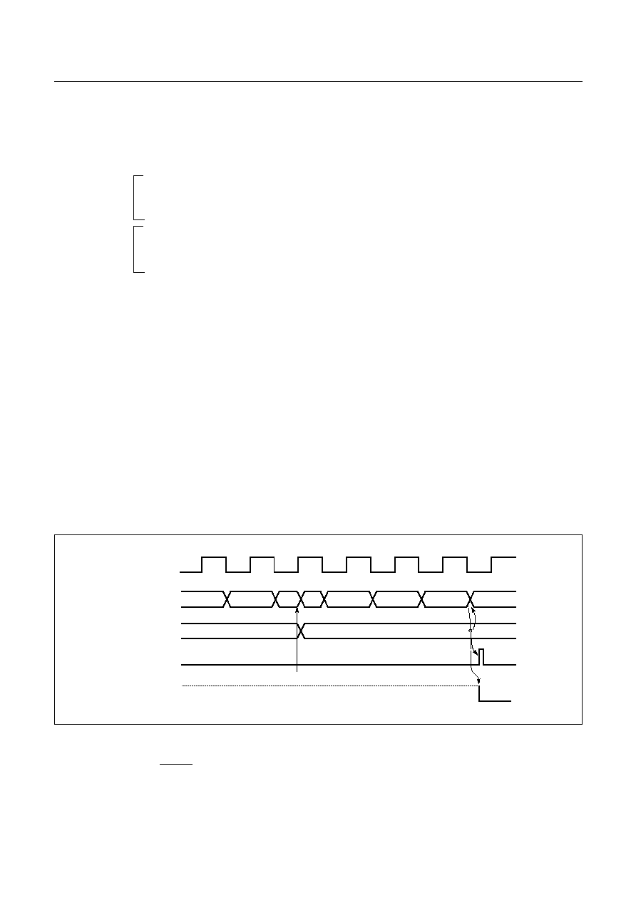
HYUNDAI MicroElectronics
GMS82512/16/24
FEB. 2000 Ver 1.00
55
Example: Sets the watchdog timer detection time to 0.5 sec at 4.19MHz
Enable and Disable Watchdog
Watchdog timer is enabled by setting WDTON (bit 5 in
CKCTLR) to "1". WDTON is initialized to "0" during re-
set and it should be set to "1" to operate after reset is re-
leased.
Example: Enables watchdog timer for Reset
:
LDM
CKCTLR,#xx1x_xxxxB;
WDTON
1
:
:
The watchdog timer is disabled by clearing bit 5 (WD-
TON) of CKCTLR. The watchdog timer is halted in STOP
mode and restarts automatically after STOP mode is re-
leased.
Watchdog Timer Interrupt
The watchdog timer can be also used as a simple 6-bit tim-
er by clearing bit5 of CKCTLR to "0". The interval of
watchdog timer interrupt is decided by Basic Interval Tim-
er. Interval equation is shown as below.
The stack pointer (SP) should be initialized before using
the watchdog timer output as an interrupt source.
Example: 6-bit timer interrupt set up.
LDM
CKCTLR,#xx0xxxxxB;
WDTON
0
LDM
WDTR,#7FH
;
WDTCL
1
:
Figure 15-3 Watchdog timer Timing
If the watchdog timer output becomes active, a reset is gen-
erated, which drives the RESET pin low to reset the inter-
nal hardware.
The main clock oscillator also turns on when a watchdog
timer reset is generated in sub clock mode.
LDM
CKCTLR,#3FH
;
Select 1/2048 clock source
,
WDTON
1, Clear Counter
LDM
WDTR,#04FH
LDM
WDTR,#04FH
;
Clear counter
:
:
:
:
LDM
WDTR,#04FH
;
Clear counter
:
:
:
:
LDM
WDTR,#04FH
;
Clear counter
Within WDT
detection time
Within WDT
detection time
T
WDTR
Interval of BIT
×
=
2
3
n
Source clock
Binary-counter
WDTR
WDTIF interrupt
WDTR
"0100_0011
B
"
1
0
Match
Detect
Counter
Clear
1
2
3
0
BIT overflow
3
WDT reset
reset
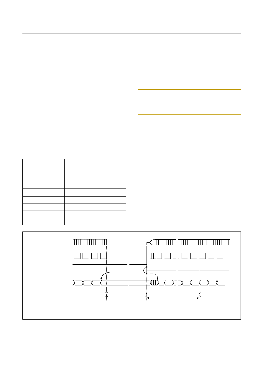
GMS82512/16/24
HYUNDAI MicroElectronics
56
FEB. 2000 Ver 1.00
16. POWER DOWN OPERATION
GMS825xx has a power-down mode. In power-down
mode, power consumption is reduced considerably that in
battery operation. Battery life can be extended a lot.
STOP Mode is entered by STOP instruction.
16.1 STOP Mode
For applications where power consumption is a critical
factor, device provides reduced power of STOP.
Start The Stop Operation
An instruction that STOP causes to be the last instruction
is executed before going into the STOP mode. In the Stop
mode, the on-chip main-frequency oscillator is stopped.
With the clock frozen, all functions are stopped, but the on-
chip RAM and Control registers are held. The port pins
output the values held by their respective port data register,
the port direction registers. The status of peripherals during
Stop mode is shown below.
Note: Since the X
IN
pin is connected internally to GND to
avoid current leakage due to the crystal oscillator in STOP
mode, do not use STOP instruction when an external clock
is used as the main system clock.
In the Stop mode of operation, V
DD
can be reduced to min-
imize power consumption. Be careful, however, that V
DD
is not reduced before the Stop mode is invoked, and that
V
DD
is restored to its normal operating level before the
Stop mode is terminated.
The reset should not be activated before V
DD
is restored to
its normal operating level, and must be held active long
enough to allow the oscillator to restart and stabilize.
And after STOP instruction, at least two or more NOP in-
struction should be written as shown in example below.
Example:
LDM
CKCTLR,#0000_1110B
STOP
NOP
NOP
:
The Interval Timer Register CKCTLR should be initial-
ized (0F
H
or 0E
H
) by software in order that oscillation sta-
bilization time should be longer than 20ms before STOP
mode.
Figure 16-1 STOP Mode Release Timing by External Interrupt
Peripheral
STOP Mode
CPU
All CPU operations are disabled
RAM
Retain
X
IN
PIN
Low
X
OUT
PIN
High
Oscillation
Stop
I/O ports
Retain
Control Registers
Retain
Release method
by RESET, by External interrupt
Before executing Stop instruction, Basic Interval Timer must be set
Oscillator
(X
IN
pin)
~~
n
0
BIT Counter
n+1
n+2
n+3
~~
Normal Operation
Stop Operation
Normal Operation
1
FE
FF
0
1
2
~~
~~
~~
t
ST
>
20ms
~~
~~
External Interrupt
Internal Clock
Clear
STOP Instruction
Executed
~~
~~
~~
properly by software to get stabilization time which is longer than 20ms.
by software
~~
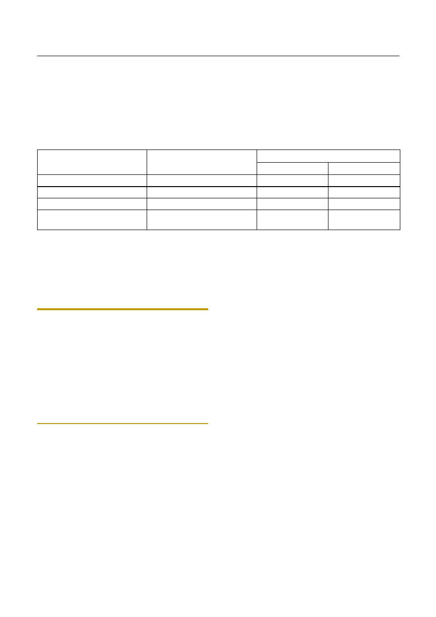
HYUNDAI MicroElectronics
GMS82512/16/24
FEB. 2000 Ver 1.00
57
Release the STOP mode
The exit from STOP mode is using hardware reset or exter-
nal interrupt.
To release STOP mode, corresponding interrupt should be
enabled before STOP mode.
Reset redefines all the control registers but does not change
the on-chip RAM. External interrupts allow both on-chip
RAM and Control registers to retain their values.
Start-up is performed to acquire the time for stabilizing os-
cillation. During the start-up, the internal operations are all
stopped.
16.2 Minimizing Current Consumption
The Stop mode is designed to reduce power consumption.
To minimize current drawn during Stop mode, the user
should turn-off output drivers that are sourcing or sinking
current, if it is practical.
Note: In the STOP operation, the power dissipation asso-
ciated with the oscillator and the internal hardware is low-
ered; however, the power dissipation associated with the
pin interface (depending on the external circuitry and pro-
gram) is not directly determined by the hardware operation
of the STOP feature. This point should be little current flows
when the input level is stable at the power voltage level
(V
DD
/V
SS
); however, when the input level becomes higher
than the power voltage level (by approximately 0.3V), a cur-
rent begins to flow. Therefore, if cutting off the output tran-
sistor at an I/O port puts the pin signal into the high-
impedance state, a current flow across the ports input tran-
sistor, requiring it to fix the level by pull-up or other means.
It should be set properly in order that current flow through
port doesn't exist.
First conseider the setting to input mode. Be sure that there
is no current flow after considering its relationship with
external circuit. In input mode, the pin impedance viewing
from external MCU is very high that the current doesn't
flow.
But input voltage level should be V
SS
or V
DD
. Be careful
that if unspecified voltage, i.e. if unfirmed voltage level
(not V
SS
or V
DD
) is applied to input pin, there can be little
current (max. 1mA at around 2V) flow.
If it is not appropriate to set as an input mode, then set to
output mode considering there is no current flow. Setting
to High or Low is decided considering its relationship with
external circuit. For example, if there is external pull-up re-
sistor then it is set to output mode, i.e. to High, and if there
Event
MCU Status before event
Chip function after event
PC
Oscillator Circuit
RESET
Don't care
Vector
on
STOP instruction
Normal operation
N +1
off
External Interrupt
Normal operation
Vector
on
External Interrupt Wake up
STOP, I flag = 1
STOP, I flag = 0
Vector
N + 1
on
on
Table 16-1 Wake-up and Reset Function Table
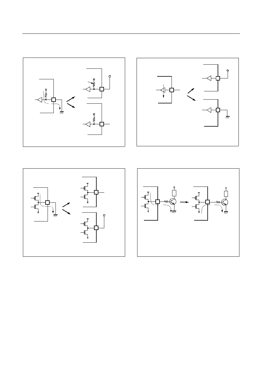
GMS82512/16/24
HYUNDAI MicroElectronics
58
FEB. 2000 Ver 1.00
is external pull-down register, it is set to low.
Figure 16-2 Application Example of Unused Input Port
Figure 16-3 Application Example of Unused Output Port
INPUT PIN
V
DD
GND
i
V
DD
X
Weak pull-up current flows
V
DD
internal
pull-up
INPUT PIN
i
V
DD
X
Very weak current flows
V
DD
O
O
OPEN
OPEN
i=0
O
i=0
O
GND
When port is configure as an input, input level should
be closed to 0V or 5V to avoid power consumption.
OUTPUT PIN
GND
i
In the left case, much current flows from port to GND.
X
ON
OFF
OUTPUT PIN
GND
i
In the left case, Tr. base current flows from port to GND.
i=0
X
OFF
ON
V
DD
L
ON
OFF
OPEN
GND
V
DD
L
ON
OFF
To avoid power consumption, there should be low output
ON
OFF
O
O
V
DD
O
to the port.
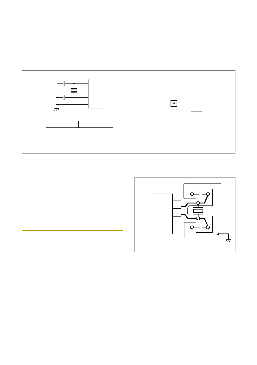
HYUNDAI MicroElectronics
GMS82512/16/24
FEB. 2000 Ver 1.00
59
17. OSCILLATOR CIRCUIT
The GMS825xx has two oscillation circuits internally. X
IN
and X
OUT
are input and output for frequency, respectively,
inverting amplifier which can be configured for being used
as an on-chip oscillator, as shown in Figure 17-1.
Figure 17-1 Oscillation Circuit
Oscillation circuit is designed to be used either with a ce-
ramic resonator or crystal oscillator. Since each crystal and
ceramic resonator have their own characteristics, the user
should consult the crystal manufacturer for appropriate
values of external components.
Oscillation circuit is designed to be used either with a ce-
ramic resonator or crystal oscillator. Since each crystal and
ceramic resonator have their own characteristics, the user
should consult the crystal manufacturer for appropriate
values of external components.
In addition, see Figure 17-2 for the layout of the crystal.
Note: Minimize the wiring length. Do not allow the wiring to
intersect with other signal conductors. Do not allow the wir-
ing to come near changing high current. Set the potential of
the grounding position of the oscillator capacitor to that of
V
SS
. Do not ground it to any ground pattern where high cur-
rent is present. Do not fetch signals from the oscillator.
Figure 17-2 Layout of Oscillator PCB circuit
X
OUT
X
IN
V
SS
Recommend
C1,C2 = 30pF±10pF
C1
C2
X
OUT
X
IN
External Clock
Open
External Oscillator
Crystal or Ceramic Oscillator
8MHz
Crystal Oscillator
X
OUT
X
IN
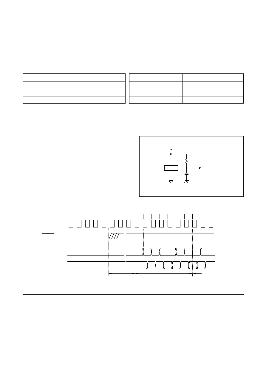
GMS82512/16/24
HYUNDAI MicroElectronics
60
FEB. 2000 Ver 1.00
18. RESET
The GMS825xx have two types of reset generation proce-
dures; one is an external reset input, the other is a watch-
dog timer reset. Table 18-1 shows on-chip hardware ini-
tialization by reset action.
Table 18-1 Initializing Internal Status by Reset Action
18.1 External Reset Input
The reset input is the RESET pin, which is the input to a
Schmitt Trigger. A reset in accomplished by holding the
RESET pin low for at least 8 oscillator periods, within the
operating voltage range and oscillation stable, it is applied,
and the internal state is initialized. After reset, 64ms (at 4
MHz) add with 7 oscillator periods are required to start ex-
ecution as shown in Figure 18-2.
Internal RAM is not affected by reset. When V
DD
is turned
on, the RAM content is indeterminate. Therefore, this
RAM should be initialized before read or tested it.
When the RESET pin input goes to high, the reset opera-
tion is released and the program execution starts at the vec-
tor address stored at addresses FFFE
H
- FFFF
H
.
A connection for simple power-on-reset is shown in Figure
18-1.
Figure 18-1 Simple Power-on-Reset Circuit
Figure 18-2 Timing Diagram after RESET
18.2 Watchdog Timer Reset
Refer to "15. WATCHDOG TIMER" on page 54.
On-chip Hardware
Initial Value
On-chip Hardware
Initial Value
Program counter
(PC)
(FFFF
H
) - (FFFE
H
)
Watchdog timer
Disable
G-flag
(G)
0
Control registers
Refer to Table 8-1 on page 22
Peripheral clock
Off
Power fail detector
Disable
7036P
V
CC
10uF
+
10k
to the RESET pin
MAIN PROGRAM
Oscillator
(X
IN
pin)
?
?
FFFE FFFF
Stabilization Time
t
ST
= 62.5mS at 4.19MHz
RESET
ADDRESS
DATA
1
2
3
4
5
6
7
?
?
Start
?
?
?
FE
?
ADL
ADH
OP
BUS
BUS
RESET Process Step
~~
~~
~~
~~
~~
~~
t
ST
=
x 256
f
MAIN
÷
1024
1
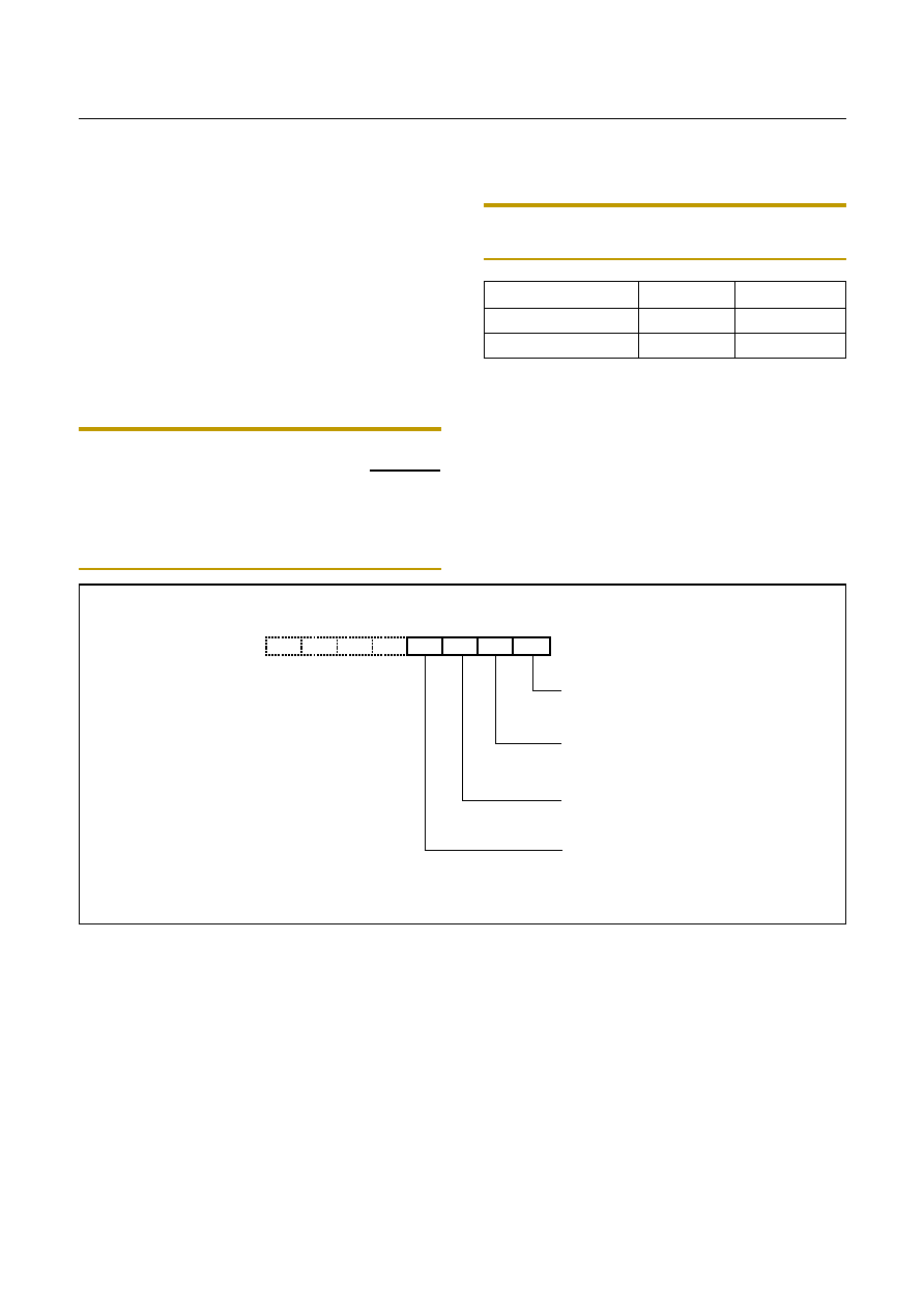
HYUNDAI MicroElectronics
GMS82512/16/24
FEB. 2000 Ver 1.00
61
19. POWER FAIL PROCESSOR
The GMS825xx has an on-chip power fail detection cir-
cuitry to immunize against power noise. A configuration
register, PFDR, can enable or disable the power fail detect
circuitry. Whenever V
DD
falls close to or below power fail
voltage for 100ns, the power fail situation may reset or
freeze MCU according to PFR bit of PFDR. Refer to "7.4
DC Electrical Characteristics" on page 11.
In the in-circuit emulator, power fail function is not imple-
mented and user can not experiment with it. Therefore, af-
ter final development of user program, this function may
be experimented or evaluated.
Note: User can select power fail voltage level according to
PFV bit of PFDR at the OTP(GMS82524T) but must select
the power fail voltage level to define PFD option of "Mask
Order & Verification Sheet" at the mask chip(GMS825xx).
Because the power fail voltage level of mask chip
(GMS825xx) is determined according to mask option re-
gardless of PFV bit of PFDR
Note: If power fail voltage is selected to 3.0V on 3V oper-
ation, MCU is freezed at all the times
.
Table 19-1 Power fail processor
Figure 19-1 Power Fail Voltage Detector Register
Power FailFunction
OTP
MASK
Enable/Disable
by PFD flag
by PFD flag
Level Selection
by PFV flag
by mask option
7
6
5
4
3
2
1
0
PFS
INITIAL VALUE: ---- 1100
B
ADDRESS: 0F9
H
PFDR
R/W
R/W
R/W
PFD
Operation Mode
0: Normal operation regardless of power fail
1: MCU will be reset by power fail detection
Disable Flag
0: Power fail detection enable
1: Power fail detection disable
Power Fail Status
0: Normal operate
1: Set to "1" if power fail is detected
PFR
PFV
Power Fail Voltage Selection Flag
0: 2.4V
1: 3.0V
R/W
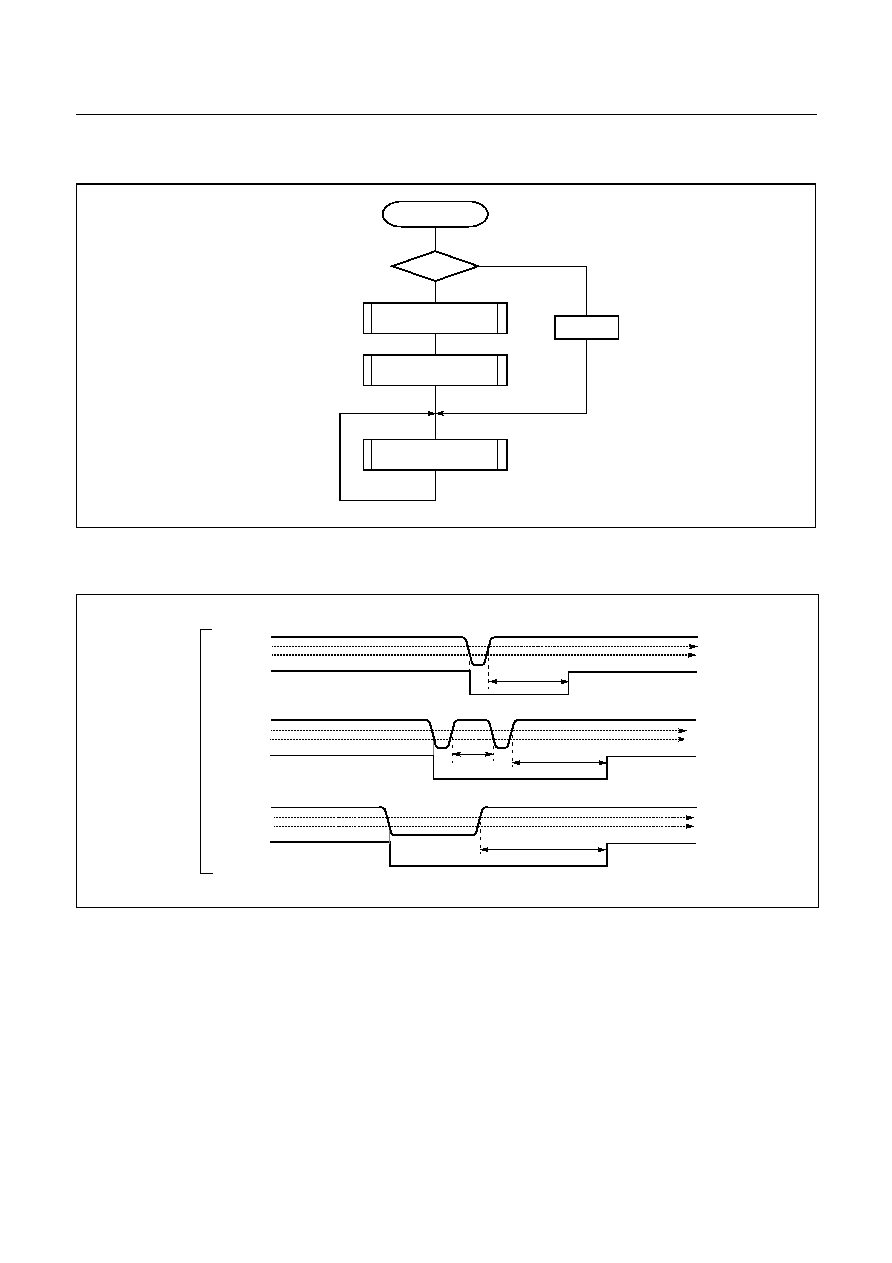
GMS82512/16/24
HYUNDAI MicroElectronics
62
FEB. 2000 Ver 1.00
Figure 19-2 Example S/W of RESET flow by Power fail
Figure 19-3 Power Fail Processor Situations
FUNTION
EXECUTION
INITIALIZE RAM DATA
PFS =1
NO
RESET VECTOR
INITIALIZE ALL PORTS
INITIALIZE REGISTERS
RAM CLEAR
YES
Skip the
initial routine
PFS = 0
Internal
RESET
Internal
RESET
Internal
RESET
V
DD
V
DD
V
DD
V
PFD
MAX
V
PFD
MIN
V
PFD
MAX
V
PFD
MIN
V
PFD
MAX
V
PFD
MIN
64mS
64mS
t <64mS
64mS
When PFR = 1
HYUNDAI MicroElectronics
GMS82512/16/24
FEB. 2000 Ver 1.00
63
20. OTP PROGRAMMING
The GMS82524T is OTP (One Time Programmable) mi-
crocontroller. Its internal user memory is constructed with
EPROM (Electrically Programmable Read Only Memo-
ry).
The OTP micorcontroller is generally used for chip evalu-
ation, first production, small amount production, fast mass
production, etc.
Blank OTP's internal EPROM is filled by 00
H
, not FF
H
.
Note: In any case, you have to use *.OTP file, not *.HEX
file. After assemble, both OTP and HEX file are generated
by automatically. The HEX file is used during porgram em-
ulation on emulator.
20.1 How to Program
To program the OTP devices, user can use HME own pro-
grammer or third party universal programmer shown as
listed below.
HME own programmer list
Manufacturer: Hyundai MicroElectronics
Programmer: Choice-Dr Writer
Choice-Sigma, Choice-Gang4
The Choice-Dr Writer is single writer and physically add-
on adapter board type, it should be used with Choice-Dr
emulator. However, the Choice-Sigma is stand alone HME
universal single programmer for any HME OTP devices,
also the Choice-Gang4 can program four OTPs at once.
Ask to HME sales part which is listed on appendix of this
manual.
Third party programmer list
Manufacturer: Hi-Lo Systems
Programmer: ALL-11, ALL-07
Website : http: //www.hilosystems.com.tw
Socket adapters are supported by third party programmer's
manufacturer. The other third party will be registered and
being under development.
Programming Procedure
1. Select device GMS82524T.
2. Load the *.OTP file to the programmer. The file is com-
posed of Motorola-S1 format.
3. Set the programming address range as below table.
4. Mount the socket adapter on the programmer.
5. Start program/verify.
20.2 Pin Function
V
PP
(Program Voltage)
V
PP
is the input for the program voltage for programming
the EPROM.
CE (Chip Enable)
CE is the input for programming and verifying internal
EPROM.
OE (Output Enable)
OE is the input of data output control signal for verify.
A0~A15 (Address Bus)
A0~A15 are address input pins for internal EPROM.
D0~D7 (EPROM Data Bus)
These are data bus for internal EPROM.
N.C. (No Connection)
GMS82524T
Address
Set Value
Bufferstart address
2000H
Buffer end address
7FFFH
Device start address
A000H
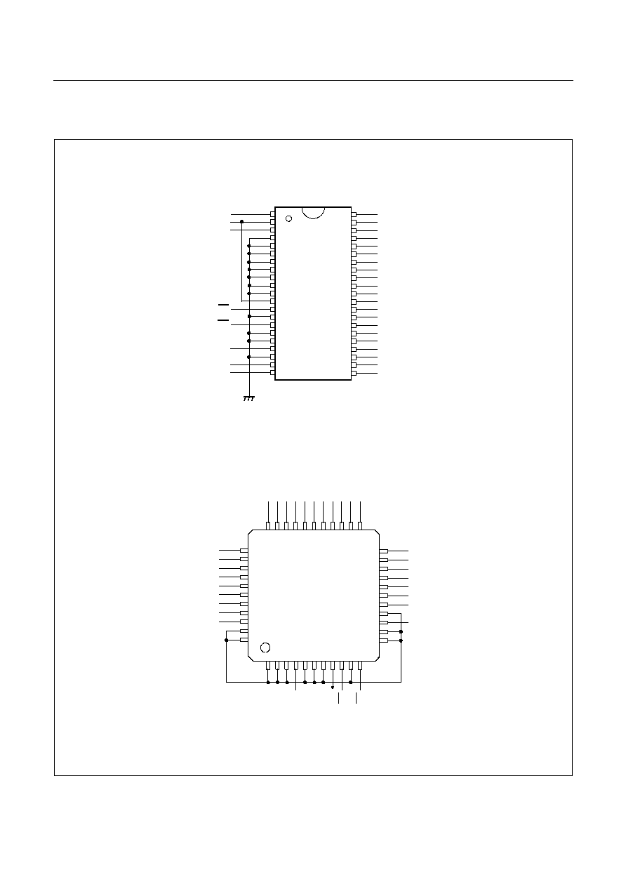
GMS82512/16/24
HYUNDAI MicroElectronics
64
FEB. 2000 Ver 1.00
A1
A2
A3
A4
A5
A6
A7
D0
D1
D2
D3
D4
D5
D6
D7
A8
A9
A10
A11
A12
A13
42SDIP
1
2
3
4
5
6
7
8
9
10
11
12
13
14
15
16
17
18
19
20
21
42
41
40
39
38
37
36
35
34
33
32
31
30
29
28
27
26
25
24
23
22
G
M
S
8
2
524T
(Top View)
A0
V
DD
V
PP
GND
CE
OE
N.C.
*
A15
A14
(Top View)
A9
A10
A11
A12
A13
A14
A15
A7
D0
D1
D2
D3
D4
D5
D6
D7
N.C.
A8
1
2
3
4
5
6
7
8
9
10
11
A6
A5
A4
A3
A2
A1
A0
V
DD
33
32
31
30
29
28
27
26
25
24
23
17
16
15
14
13
12
34
35
36
37
38
39
40
41
42
43
44
GMS82524T
44QFP
18
19
20
21
22
N.C.
*
V
PP
CE
OE
V
DD
N.C.
*
N.C.
*
: No Connection
HYUNDAI MicroElectronics
GMS82512/16/24
FEB. 2000 Ver 1.00
65
20.3 Programming Specification
DEVICE OPERATION MODE
(T
A
= 25
°
C ± 5
°
C)
DEVICE CHARACTERISTICS
(V
SS
=0V, T
A
= 25
°
C ± 5
°
C)
Mode
CE
OE
A0~A15
V
PP
V
DD
O0~O7
Read Mode
X
1
X
1
V
DD
2
5.0V
DOUT
Output Disable Mode
V
IH
V
IH
X
1
V
DD
2
5.0V
Hi-Z
Programming Mode
V
IL
V
IH
X
1
V
PP
2
V
DD
2
DIN
Program Verify
X
1
X
1
V
PP
2
V
DD
2
DOUT
1. X = Either V
IL
or V
IH
.
2. See DC Characteristics Table for V
DD
and V
PP
voltage during programming.
Symbol
Item
Min
Typ
Max
Unit
Test condition
V
PP
Quick Pulse Programming
11.50
11.75
12.0
V
V
DD
1
Quick Pulse Programming
5.75
6.0
6.25
V
I
PP
2
V
PP
supply current
50
mA
CE=V
IL
I
DD
2
V
DD
supply current
30
mA
V
IH
Input high voltage
0.8V
DD
V
V
IL
Input low voltage
0.2V
DD
V
V
OH
Output high voltage
V
DD
-0.1
V
I
OH
= -2.5mA
V
OL
Output low voltage
0.4
V
I
OL
= 2.1mA
I
IL
Input leakage current
5
µ
A
1. V
DD
must be applied simultaneously or before V
PP
and removed simultaneously or after V
PP
.
2. The maximum current value is with outputs O0 to O7 unloaded.
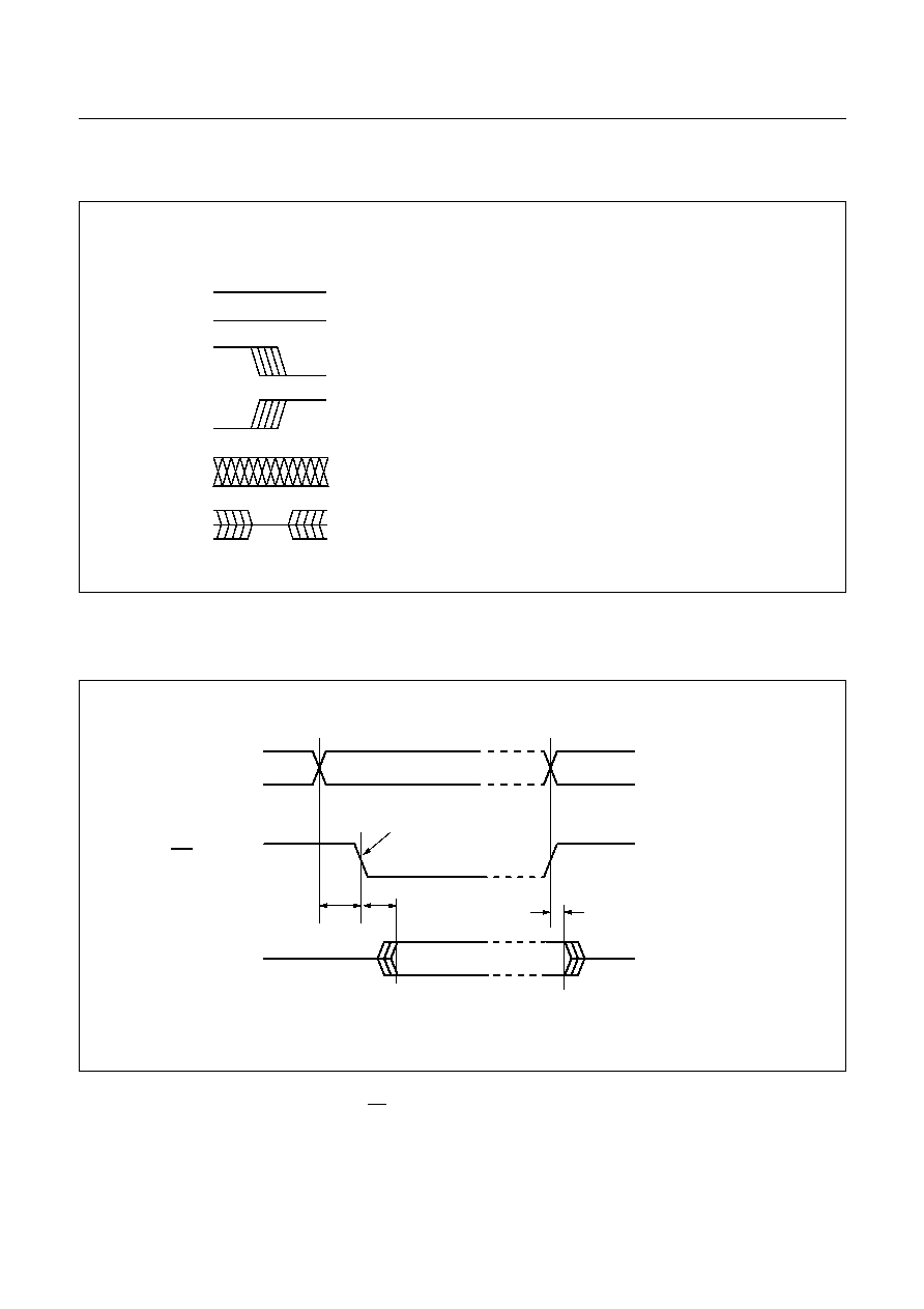
GMS82512/16/24
HYUNDAI MicroElectronics
66
FEB. 2000 Ver 1.00
SWITCHING WAVEFORMS
READING WAVEFORMS
1. The input timing reference level is 1.0V for a V
IL
and 4.0V for a V
IH
at V
DD
=5.0V.
2. To read the output data, transition requires on the OE form the high to the low after address setup time t
AS
.
WAVEFORM
Must be steady
INPUTS
OUTPUTS
Will be steady
May change
Will be changing
from H to L
from H to L
May change
Will be changing
from L to H
from L to H
Do not care any
Changing state
change permitted
unknown
Does not apply
Center line is
high impedance "Off" state
Addresses Valid
Addresses
Valid Output
V
IH
V
IL
V
IH
V
IL
V
IH
V
IL
OE
Output
t
AS
t
OE
t
DH
High-Z
See note (2)
HYUNDAI MicroElectronics
GMS82512/16/24
FEB. 2000 Ver 1.00
67
PROGRAMMING ALGORITHM WAVEFORMS
1. The input timing reference level is 1.0V for a V
IL
and 4.0V for a V
IH
at V
DD
=5.0V.
Addresses Valid
Addresses
V
IH
V
IL
t
DH
High-Z
t
AH
t
DFP
Program
Program
Verify
Data In/Out
V
PP
V
DD
CE
OE
t
AS
t
DS
t
VPS
t
VDS
t
PW
Data in Stable
Data out valid
t
OES
t
OE
V
IH
V
IL
12.75V
V
DD
6.25V
5.0V
V
IH
V
IL
V
IH
V
IL

GMS82512/16/24
HYUNDAI MicroElectronics
68
FEB. 2000 Ver 1.00
AC READING CHARACTERISTICS
(V
SS
=0V, T
A
= 25
°
C ± 5
°
C)
Note: V
DD
must be applied simultaneously or before V
PP
and removed simultaneously or after V
PP
.
AC PROGRAMMING CHARACTERISTICS
(V
SS
=0V, T
A
= 25
°
C ± 5
°
C)
* AC CONDITION OF TEST
Input Rise and Fall Times (10% to 90%) ........................... 20ns
Input Pulse Levels ............................................................. 0.45V to 4.55V
Input Timing Reference Level............................................ 1.0V to 4.0V
Output Timing Reference Level ......................................... 1.0V to 4.0V
V
DD
must be applied simultaneously or before V
PP
and removed simultaneously or after V
PP
.
Symbol
Item
Min
Typ
Max
Unit
Test condition
t
AS
Address setup time
2
µ
s
t
OE
Quick Pulse Programming
200
ns
t
DH
V
PP
supply current
0
50
ns
Symbol
Item
Min
Typ
Max
Unit
Test condition*
t
AS
Address setup time
2
µ
s
t
OES
OE setup time
2
µ
s
t
DS
Data setup time
2
µ
s
t
AH
Address hold time
0
µ
s
t
DH
Data hold time
2
µ
s
t
DFP
Output delay disable time
0
130
ns
t
VPS
V
PP
setup time
2
µ
s
t
VDS
V
DD
setup time
2
µ
s
t
PW
Program pulse width
95
100
105
µ
s
t
OE
Data output delay time
150
ns
HYUNDAI MicroElectronics
GMS82512/16/24
FEB. 2000 Ver 1.00
69
Table 20-1 Programming Algorithm
START
ADDRESS=FIRST LOCATION
V
CC
=6.0V
5V
V
PP
=11.75
5V
X=0
PROGRAM ONE 100
µ
s PULSE
INCREMENT X
X=25?
NO
YES
VERIFY
ONE BYTE
LAST
ADDRESS?
V
CC
=V
PP
=5.0V
COMPARE
ALL BYTES TO
ORIGINAL
DATA
DEVICE
FAILED
DEVICE
PASSED
VERIFY
BYTE
INCREMENT
ADDRESS
NO
YES
FAIL
PASS
FAIL
PASS
FAIL
PASS

APPENDIX
GMS82512/16/24
HYUNDAI MicroElectronics
i
FEB. 2000 Ver 1.00
A. CONTROL REGISTER LIST
Address
Register Name
Symbol
R/W
Initial Value
Page
7 6 5 4 3 2 1 0
00C0
R0 port data register
R0
R/W
Undefined
page 28
00C1
R0 port I/O direction register
R0DD
W
0 0 0 0 0 0 0 0
page 28
00C4
R2 port data register
R2
R/W
Undefined
page 28
00C5
R2 port I/O direction register
R2DD
W
0 0 0 0 0 0 0 0
page 28
00C6
R3 port data register
R3
R/W
Undefined
page 28
00C7
R3 port I/O direction register
R3DD
W
0 0 0 0 0 0 0 0
page 28
00C8
R4 port data register
R4
R/W
Undefined
page 29
00C9
R4 port I/O direction register
R4DD
W
- - - 0 0 0 0 0
page 29
00CA
R5 port data register
R5
R/W
Undefined
page 30
00CB
R5 port I/O direction register
R5DD
W
- - 0 0 - - - -
page 30
00CC
R6 port data register
R6
R/W
Undefined
page 30
00CD
R6 port I/O direction register
R6DD
W
0 0 0 0 - - - -
page 30
00D0
R4 port mode register
PMR4
W
- - - 0 0 0 0 0 page 29, page 53
00D1
R5 port mode register
PMR5
W
- - 0 0 - - - - page 30, page 45
00D3
Basic interval timer mode register
BITR
R
Undefined
page 32
Clock control register
CKCTLR
W
- - 0 1 0 1 1 1
page 32
00E0
Watchdog Timer Register
WDTR
W
- 0 1 1 1 1 1 1
page 54
00E2
Timer mode register 0
TM0
R/W
0 0 0 0 0 0 0 0
page 34
00E3
Timer mode register 2
TM2
R/W
0 0 0 0 0 0 0 0
page 34
00E4
Timer 0 data register
TDR0
W
Undefined
page 34
Timer 0 counter register
T0
R
Undefined
page 34
00E5
Timer 1 data register
TDR1
W
Undefined
page 34
Timer 1 counter register
T1
R
Undefined
page 34
00E6
Timer 2 data register
TDR2
W
Undefined
page 34
Timer 2 counter register
T2
R
Undefined
page 34
00E7
Timer 3 data register
TDR3
W
Undefined
page 34
Timer 3 counter register
T3
R
Undefined
page 34
00E8
A/D converter mode register
ADCM
R/W
- - 0 0 0 0 0 1
page 44
00E9
A/D converter data register
ADR
R
Undefined
page 44
00EC
Buzzer driver register
BUR
W
Undefined
page 45
00F4
Interrupt enable register low
IENL
R/W
0 0 0 - - - - -
page 48
00F5
Interrupt request flag register low
IRQL
R/W
0 0 0 - - - - -
page 47
00F6
Interrupt enable register high
IENH
R/W
0 0 0 0 0 0 0 0
page 48
00F7
Interrupt request flag register high
IRQH
R/W
0 0 0 0 0 0 0 0
page 47
00F8
External interrupt edge selection register
IEDS
W
0 0 0 0 0 0 0 0
page 53
00F9
Power fail detection register
PFDR
R/W
- - - - 1 1 0 0
page 61
HYUNDAI MicroElectronics
GMS82512/16/24
FEB. 2000 Ver 1.00
ii
B. SOFTWARE EXAMPLE
B.1 7-segment LED display
;*****************************************************************************
; Title: GMS82516 (GMS800 Series) Demonstration Program *
; Company: HYUNDAI Micro Electronics *
; Contents: Decimal Up/Down Counter *
; Programmer: HME MCU application team *
;*****************************************************************************
;
;******** DEFINE I/O PORT & FUNCTION REGISTER ADDRESS *********
;
R0 EQU 0C0H ;port R0 register
R0DD EQU 0C1H ;port R0 data I/O direction register
;
R2 EQU 0C4H ;port R2 register
R2DD EQU 0C5H ;port R2 data I/O direction register
;
R3 EQU 0C6H ;port R3 register
R3DD EQU 0C7H ;port R3 data I/O direction register
;
R4 EQU 0C8H ;port R4 register
R4DD EQU 0C9H ;port R4 data I/O direction register
;
R5 EQU 0CAH ;port R5 register
R5DD EQU 0CBH ;port R5 data I/O direction register
;
R6 EQU 0CCH ;port R6 register
R6DD EQU 0CDH ;port R6 data I/O direction register
;
PMR4 EQU 0D0H ;port R4 mode register
EC0S EQU 4,0D0H ;event counter 0 selection
INT3S EQU 3,0D0H ;external int.3 selection
INT2S EQU 2,0D0H ;external int.2 selection
INT1S EQU 1,0D0H ;external int.1 selection
GMS82512/16/24
LED Display
GND
R00
R01
R02
R03
R04
R05
R06
a
b
c
d
e
f
g
330
×
7
4.7k
4.7k
R23
R22
R20/INT0
R21/INT1
UP/DOWN S/W
CLEAR S/W
2N2222
2N2222
V
DD
TEST
5V
5V
GND
V
SS

GMS82512/16/24
HYUNDAI MicroElectronics
iii
FEB. 2000 Ver 1.00
INT0S EQU 0,0D0H ;external int.0 selection
;
PMR5 EQU 0D1H ;port R5 mode register
BUZS EQU 5,0D1H ;buzzer selection
WDTS EQU 4,0D1H ;watch dog timer selection
;
CKCTLR EQU 0D3H ;clock control register
BITR EQU 0D3H ;basic interval timer register
;
WDTR EQU 0E0H ;watch dog timer register
;
TM0 EQU 0E2H ;timer0 mode register
TM2 EQU 0E3H ;timer2 mode register
;
TDR0 EQU 0E4H ;tomer0 data register
TDR1 EQU 0E5H ;tomer1 data register
TDR2 EQU 0E6H ;tomer2 data register
TDR3 EQU 0E7H ;tomer3 data register
;
ADCM EQU 0E8H ;A/D Converter mode register
ADR EQU 0E9H ;A/D con. register
;
BUR EQU 0ECH ;buzzer data register
;
IENL EQU 0F4H ;int. enable register low
AE EQU 7,0F4H ;A/D con. int. enable
WDTE EQU 6,0F4H ;W.D.T. int. enable
BITE EQU 5,0F4H ;B.I.T. int. enable
;
IRQL EQU 0F5H ;int. request flag register low
AR EQU 7,0F5H ;A/D con. int. request flag
WDTRF EQU 6,0F5H ;W.D.T. int. request flag
BITRF EQU 5,0F5H ;B.I.T. int. request flag
;
IENH EQU 0F6H ;int. enable register high
INT0E EQU 7,0F6H ;external int.0 enable
INT1E EQU 6,0F6H ;external int.1 enable
INT2E EQU 5,0F6H ;external int.2 enable
INT3E EQU 4,0F6H ;external int.3 enable
T0E EQU 3,0F6H ;timer0 int. enable
T1E EQU 2,0F6H ;timer1 int. enable
T2E EQU 1,0F6H ;timer2 int. enable
T3E EQU 0,0F6H ;timer3 int. enable
;
IRQH EQU 0F7H ;int. request flag register high
INT0R EQU 7,0F7H ;external int.0 request flag
INT1R EQU 6,0F7H ;external int.1 request flag
INT2R EQU 5,0F7H ;external int.2 request flag
INT3R EQU 4,0F7H ;external int.3 request flag
T0R EQU 3,0F7H ;timer0 int. request flag
T1R EQU 2,0F7H ;timer1 int. request flag
T2R EQU 1,0F7H ;timer2 int. request flag
T3R EQU 0,0F7H ;timer3 int. request flag
;
IEDS EQU 0F8H ;external int. edge selection
PFDR EQU 0F9H ;power fail detection register
;
;*********** MACRO DEFINITION ************
;
REG_SAVE MACRO ;Save Registers to Stacks
PUSH A
PUSH X
PUSH Y
ENDM
;
REG_RESTORE MACRO ;Restore Register from Stacks
POP Y
POP X
POP A
ENDM
;
;*********** CONSTANT DEFINITION ***********
;
SEG_PORT EQU R0 ;7-Segment Output Port
STROBE_PORT EQU R2 ;Strobe Signal Port
;
;**************************************************************************
; RAM ALLOCATION *
;**************************************************************************

HYUNDAI MicroElectronics
GMS82512/16/24
FEB. 2000 Ver 1.00
iv
DIGIT10 DS 1 ;DIG10 Display Data
DIGIT1 DS 1 ;Seg1 Display Data
STROBE DS 1 ;Strobe Signal Data
TMR_500mS DS 1 ;500ms Time Counter
FLAGS DS 1 ;Function Flags
UP_F EQU 0,FLAGS ;1=Down,0=Up
F_500ms EQU 1,FLAGS ;
;
;**************************************************************************
; INTERRUPT VECTOR TABLE *
;**************************************************************************
;
ORG0FFE4H
DW NOT_USED ; Serial I/O
DW NOT_USED ; Basic Interval Timer
DW NOT_USED ; Watch Dog Timer
DW NOT_USED ; A/D CON.
DW NOT_USED ; Timer-3
DW NOT_USED ; Timer-2
DW NOT_USED ; Timer-1
DW TMR0_INT ; Timer-0
DW NOT_USED ; Int.3
DW NOT_USED ; Int.2
DW INT_1 ; Int.1
DW INT_0 ; Int.0
DW NOT_USED ;
DW RESET ; Reset
;
;**************************************************************************
; MAIN PROGRAM *
;**************************************************************************
;
ORG 0C000H ;Program Start Address
;
RESET: DI ;Disable All Interrupts
LDX #0
RAM_CLR: LDA #0 ;RAM Clear(!0000H->!00BFH)
STA {X}+ ;M(X) <- A, then X <- X+1
CMPX #0C0H ;X = #0C0H ?
BNE RAM_CLR
;
LDX #0FEH ;Stack Pointer Initial
TXSP ;SP. <- #0FEH
LDM R0,#0 ;I/O Port Data Clear
LDM R2,#0
LDM R0DD,#0FFH ;7-Seg. Data Output Mode
LDM R2DD,#00FH ;7-Seg. Strobe Output Mode
LDM STROBE,#0000_1011B
LDM TDR0,#250 ;8us x 250 = 2000us
LDM TM0,#0001_1111B ;Timer0(8bit),8us,Start Count-up
LDM IRQH,#0 ;Clear All Interrupts Requeat Flags
LDM IRQL,#0
LDM IENH,#1100_1000B ;EnableT0,Int0,Int1,Interrupt
LDM IENL,#00H
LDM IEDS,#0101_0101B ;External Int. Falling edge select
LDM PMR4,#03H ;General port OR Int?
SET1 UP_F
EI ;Enable Interrupts
;
Loop: nop
IF F_500ms == 1
clr1 F_500ms
call INC_DEC
ENDIF
jmp Loop
;
;***********************************************
; Subject: Inc. or Dec. two digits *
;***********************************************
; Entry: UP_F *
; Return: UP_F=1, Increment two digits *
; UP_F=0, Decrement two digits *
;***********************************************
;
INC_DEC: BBC UP_F,DOWN ;Check Down mode or Up mode
;

GMS82512/16/24
HYUNDAI MicroElectronics
v
FEB. 2000 Ver 1.00
;**************************
;* Up Count *
;**************************
;
SETC
LDA #0 ; DIGIT1 <- DIGIT1 + 1
ADC DIGIT1
IF A == #0AH
setc
lda #0
ENDIF
STA DIGIT1 ; Store result into DIGIT1
;
LDA #0 ; When Overflow is set,
ADC DIGIT10 ; DIGIT10 <- DIGIT10 + 1
IF A == #10
lda #0
ENDIF
STA DIGIT10
RET
;
;**************************
;* Down Count *
;**************************
;
DOWN: clrc
lda DIGIT1 ; DIGIT1 <- DIGIT1 - 1
sbc #0
IF A == #0FFH
lda #9
clrc
ELSE
setc
ENDIF
sta DIGIT1 ; Store result into DIGIT1
;
lda DIGIT10 ; When Overflow is set,
sbc #0 ; DIGIT10 <- DIGIT10 - 1
IF A == #0FFH
lda #9
ENDIF
STA DIGIT10
RET
;
;**************************************************************************
; TIMER0,INTERRUPT ROUTINE(2ms)& INT0,INT1 *
;**************************************************************************
;
TMR0_INT:
REG_SAVE ;Save Registers to Stacks
CALL DSPLY ;Segments Data Port Output
CALL Make_500msFalg ;250ms mesurement
REG_RESTORE ;Restore Registers from Stacks
RETI
;
;**************************************************************************
; EXTERNAL INTERRUPT 0 (UP/DOWN KEY) *
;**************************************************************************
;
INT_0: NOT1 UP_F ;INT0 Service routine
RETI ;Toggle the Up/Down mode
;
;**************************************************************************
; EXTERNAL INTERRUPT 1 (CLEAR KEY) *
;**************************************************************************
;
INT_1: LDM DIGIT1,#0 ;INT1 Service routine
LDM DIGIT10,#0
LDM TMR_500MS,#0 ;0.5Sec Restart
RETI
;
;***********************************************************************
; Subject: Seven Segment Display (DSPLY) *
;***********************************************************************
; Entry: DIGIT10 or DIGIT1 *
; Return: Output SEG_PORT (R00~R07), *
; Strobe_port (R22,R23) *
; Scratch: STROBE *
;***********************************************************************
; Description: After read internal RAM data, output data to the port *

HYUNDAI MicroElectronics
GMS82512/16/24
FEB. 2000 Ver 1.00
vi
;***********************************************************************
;
DSPLY: LDM STROBE_PORT,#03H ;Segment All Turn Off
NOT1 STROBE.2 ;Toggle strobe0
NOT1 STROBE.3 ;Toggle strobe1
IF STROBE.3 = 1 ;Test if R23 is high.
ldy DIGIT1
ELSE
ldy DIGIT10
ENDIF
LDA !FONT+Y
STA SEG_PORT ;Segment Data output
LDA STROBE
STA STROBE_PORT ;Current Digit Turn On
RET ;Quit
;
;***********************************************
; Subject: Set falg at every 500ms *
;***********************************************
; Entry: None *
; Return: 500ms flag (F_500ms) *
;***********************************************
;
Make_500msFalg:
INC TMR_500MS ;count up every 2ms
LDA TMR_500MS
IF A == #250 ;Compare 0.5S
ldm TMR_500MS,#0 ;clear 0.5sec. counter
set1 F_500ms ;set 0.5sec. flag
ENDIF
RET
;
;**************************************************************************
; 7-SEGMENT PATTERN DATA *
; _a_ *
; f | g |b *
; |---| *
; e |___|c *
; d .h *
;**************************************************************************
; Segment: hgfe dcba To be displayed Digit Number
FONT DB 0011_1111B ; 0
DB 0000_0110B ; 1
DB 0101_1011B ; 2
DB 0100_1111B ; 3
DB 0110_0110B ; 4
DB 0110_1101B ; 5
DB 0111_1100B ; 6
DB 0000_0111B ; 7
DB 0111_1111B ; 8
DB 0110_0111B ; 9
;
;**************************************************************************
;
NOT_USED: nop ;Discard Unexpected Interrupts
reti
;
END ;Notice Program End
GMS82512/16/24
HYUNDAI MicroElectronics
vii
FEB. 2000 Ver 1.00
C. INSTRUCTION
C.1 Terminology List
Terminology
Description
A
A - Register
X
X - Register
Y
Y - Register
PSW
Program Status Word
C
Carry Flag of PSW
V
Overflow Flag of PSW
N
Negative Flag of PSW
I
Master Interrupt Enable Flag of PSW
Z
Zero Flag of PSW
H
Half Carry Flag of PSW
B
Break Flag of PSW (software interrupt)
G
G flag of PSW(Direct Page)
PC
Program Counter
SP
Stack Pointer
#imm
8-Bit Immediate Data
dp
Direct Page Offset Address
!abs
Absolute Address
[ ]
Indirect Address
{ }
Register Indirect Address
{ }+
Register Indirect Address, Register Auto-Increment
.bit
Bit Position
A.bit
Bit Position of A-Register
dp.bit
Bit Position of Direct Page Memory
M.bit
Bit Position of Memory (000
H
~ 0FFF
H
)
rel
Relative Addressing Data
upage
U - Page(0FF00
H
~ 0FFFF
H
) Offset Address
n
Table CALL Number (0 ~ 15)
x
Indicate Upper Nibble of OP code
y
Indicate Upper Nibble of OP code
Assignment / Transfer / Shift Left
Shift Right
Exchange
H,h
Hexadecimal
D,d
Decimal
B,b
Binary
( )
Contents of
+
Addition
-
Subtraction
x
Multiplication
/
Division
=
Equal
Not Equal
Logical AND
v
Logical OR
Exclusive OR
(overline)
Logical NOT
Bit Position
0
Bit Position
1
HYUNDAI MicroElectronics
GMS82512/16/24
FEB. 2000 Ver 1.00
viii
C.2 Instruction Map
LOW
00000
00
00001
01
00010
02
00011
03
00100
04
00101
05
00110
06
00111
07
01000
08
01001
09
01010
0A
01011
0B
01100
0C
01101
0D
01110
0E
01111
0F
HIGH
000
-
SET1
dp.bit
BBS
A.bit,rel
BBS
dp.bit,rel
ADC
#imm
ADC
dp
ADC
dp+X
ADC
!abs
ASL
A
ASL
dp
TCALL
0
SETA1
.bit
BIT
dp
POP
A
PUSH
A
BRK
001
CLRC
//
//
//
SBC
#imm
SBC
dp
SBC
dp+X
SBC
!abs
ROL
A
ROL
dp
TCALL
2
CLRA1
.bit
COM
dp
POP
X
PUSH
X
BRA
rel
010
CLRG
//
//
//
CMP
#imm
CMP
dp
CMP
dp+X
CMP
!abs
LSR
A
LSR
dp
TCALL
4
NOT1
M.bit
TST
dp
POP
Y
PUSH
Y
PCALL
Upage
011
DI
//
//
//
OR
#imm
OR
dp
OR
dp+X
OR
!abs
ROR
A
ROR
dp
TCALL
6
OR1
OR1B
CMPX
dp
POP
PSW
PUSH
PSW
RET
100
CLRV
//
//
//
AND
#imm
AND
dp
AND
dp+X
AND
!abs
INC
A
INC
dp
TCALL
8
AND1
AND1B
CMPY
dp
CBNE
dp+X
TXSP
INC
X
101
SETC
//
//
//
EOR
#imm
EOR
dp
EOR
dp+X
EOR
!abs
DEC
A
DEC
dp
TCALL
10
EOR1
EOR1B
DBNE
dp
XMA
dp+X
TSPX
DEC
X
110
SETG
//
//
//
LDA
#imm
LDA
dp
LDA
dp+X
LDA
!abs
TXA
LDY
dp
TCALL
12
LDC
LDCB
LDX
dp
LDX
dp+Y
XCN
DAS
111
EI
//
//
//
LDM
dp,#imm
STA
dp
STA
dp+X
STA
!abs
TAX
STY
dp
TCALL
14
STC
M.bit
STX
dp
STX
dp+Y
XAS
STOP
LOW
10000
10
10001
11
10010
12
10011
13
10100
14
10101
15
10110
16
10111
17
11000
18
11001
19
11010
1A
11011
1B
11100
1C
11101
1D
11110
1E
11111
1F
HIGH
000
BPL
rel
CLR1
dp.bit
BBC
A.bit,rel
BBC
dp.bit,rel
ADC
{X}
ADC
!abs+Y
ADC
[dp+X]
ADC
[dp]+Y
ASL
!abs
ASL
dp+X
TCALL
1
JMP
!abs
BIT
!abs
ADDW
dp
LDX
#imm
JMP
[!abs]
001
BVC
rel
//
//
//
SBC
{X}
SBC
!abs+Y
SBC
[dp+X]
SBC
[dp]+Y
ROL
!abs
ROL
dp+X
TCALL
3
CALL
!abs
TEST
!abs
SUBW
dp
LDY
#imm
JMP
[dp]
010
BCC
rel
//
//
//
CMP
{X}
CMP
!abs+Y
CMP
[dp+X]
CMP
[dp]+Y
LSR
!abs
LSR
dp+X
TCALL
5
MUL
TCLR1
!abs
CMPW
dp
CMPX
#imm
CALL
[dp]
011
BNE
rel
//
//
//
OR
{X}
OR
!abs+Y
OR
[dp+X]
OR
[dp]+Y
ROR
!abs
ROR
dp+X
TCALL
7
DBNE
Y
CMPX
!abs
LDYA
dp
CMPY
#imm
RETI
100
BMI
rel
//
//
//
AND
{X}
AND
!abs+Y
AND
[dp+X]
AND
[dp]+Y
INC
!abs
INC
dp+X
TCALL
9
DIV
CMPY
!abs
INCW
dp
INC
Y
TAY
101
BVS
rel
//
//
//
EOR
{X}
EOR
!abs+Y
EOR
[dp+X]
EOR
[dp]+Y
DEC
!abs
DEC
dp+X
TCALL
11
XMA
{X}
XMA
dp
DECW
dp
DEC
Y
TYA
110
BCS
rel
//
//
//
LDA
{X}
LDA
!abs+Y
LDA
[dp+X]
LDA
[dp]+Y
LDY
!abs
LDY
dp+X
TCALL
13
LDA
{X}+
LDX
!abs
STYA
dp
XAY
DAA
111
BEQ
rel
//
//
//
STA
{X}
STA
!abs+Y
STA
[dp+X]
STA
[dp]+Y
STY
!abs
STY
dp+X
TCALL
15
STA
{X}+
STX
!abs
CBNE
dp
XYX
NOP
GMS82512/16/24
HYUNDAI MicroElectronics
ix
FEB. 2000 Ver 1.00
C.3 Alphabetic order table of instruction
NO.
MNENONIC
OP
CODE
BYTE
NO.
CYCLE
NO
OPERATION
FLAG
NVGBHIZC
1
ADC #imm
04
2
2
Add with carry.
NV - - H - ZC
2
ADC dp
05
2
3
A
A + (M) + C
3
ADC dp + X
06
2
4
4
ADC !abs
07
3
4
5
ADC !abs+Y
15
3
5
6
ADC [dp+X]
16
2
6
7
ADC [dp]+Y
17
2
6
8
ADC {X}
14
1
3
9
ADDW dp
1D
2
5
16-bits add without carry : YA
YA + (dp+1)(dp)
NV - - H - ZC
10
AND #imm
84
2
2
Logical AND
N - - - - - Z -
11
AND dp
85
2
3
A
A
(M)
12
AND dp + X
86
2
4
13
AND !abs
87
3
4
14
AND !abs+Y
95
3
5
15
AND [dp+X]
96
2
6
16
AND [dp] + Y
97
2
6
17
AND {X}
94
1
3
18
AND1 M.bit
8B
3
4
Bit AND C-flag : C
C
(M.bit)
- - - - - - - C
19
AND1B M.bit
8B
3
4
Bit AND C-flag and NOT : C
C
(
M.bit
)
- - - - - - - C
20
ASL A
08
1
2
Arithmetic shift left
N - - - - - ZC
21
ASL dp
09
2
4
22
ASL dp + X
19
2
5
23
ASL !abs
18
3
5
24
BBC A.bit,rel
y2
2
4/6
Branch if bit clear :
- - - - - - - -
25
BBC dp.bit,rel
y3
3
5/7
if(bit) = 0, then PC
PC + rel
26
BBS A.bit,rel
x2
2
4/6
Branch if bit clear :
- - - - - - - -
27
BBS dp.bit,rel
x3
3
5/7
if(bit) = 1, then PC
PC + rel
28
BCC rel
50
2
2/4
Branch if carry bit clear :
if(C) = 0, then PC
PC + rel
MM - - - - Z -
29
BCS rel
D0
2
2/4
Branch if carry bit set : If (C) =1, then PC
PC + rel
- - - - - - - -
30
BEQ rel
F0
2
2/4
Branch if equal : if (Z) = 1, then PC
PC + rel
- - - - - - - -
31
BIT dp
0C
2
4
Bit test A with memory :
MM - - - - Z -
32
BIT !abs
1C
3
5
Z
A
M, N
(M
7
), V
(M
6
)
33
BMI rel
90
2
2/4
Branch if munus : if (N) = 1, then PC
PC + rel
- - - - - - - -
34
BNE rel
70
2
2/4
Branch if not equal : if (Z) = 0, then PC
PC + rel
- - - - - - - -
35
BPL rel
10
2
2/4
Branch if not minus : if (N) = 0, then PC
PC + rel
- - - - - - - -
36
BRA rel
2F
2
4
Branch always : PC
PC + rel
- - - - - - - -
37
BRK
0F
1
8
Software interrupt:
- - - 1 - 0 - -
B
"1", M(SP)
(PC
H
), SP
SP - 1,
M(s)
(PC
L
), SP
S - 1, M(SP)
PSW,
SP
SP - 1, PC
L
(0FFDE
H
), PC
H
(0FFDF
H
)
38
BVC rel
30
2
2/4
Branch if overflow bit clear :
- - - - - - - -
If (V) = 0, then PC
PC + rel
39
BVS rel
B0
2
2/4
Branch if overflow bit set :
- - - - - - - -
If (V) = 1, then PC
PC + rel
C 7 6 5 4 3 2 1 0
"
0
"
HYUNDAI MicroElectronics
GMS82512/16/24
FEB. 2000 Ver 1.00
x
40
CALL !abs
3B
3
8
Subroutine call
- - - - - - - -
41
CALL [dp]
5F
2
8
M(SP)
(PC
H
), SP
SP-1, M(SP)
(PC
L
), SP
SP-1
if !abs, PC
abs ; if [dp], PC
L
(dp), PC
H
(dp+1)
42
CBNE dp,rel
FD
3
5/7
Compare and branch if not equal ;
- - - - - - - -
43
CBNE dp + X,
rel
8D
3
6/8
If A
(M), then PC
PC + rel.
44
CLR1 dp.bit
y1
2
4
Clear bit : (M.bit)
"0"
- - - - - - - -
45
CLR1A A.bit
2B
2
2
Clear A.bit : (A.bit)
"0"
- - - - - - - -
46
CLRC
20
1
2
Clear C-flag : C
"0"
- - - - - - - 0
47
CLRG
40
1
2
Clear G-flag : G
"0"
- - 0 - - - - -
48
CLRV
80
1
2
Clear V-flag : V
"0"
- 0 - - 0 - - -
49
CMP #imm
44
2
2
Compare accumulator contents with memory contents
N - - - - - ZC
50
CMP dp
45
2
3
A - (M)
51
CMP dp + X
46
2
4
52
CMP !abs
47
3
4
53
CMP !abs + Y
55
3
5
54
CMP [dp + X]
56
2
6
55
CMP [dp] + Y
57
2
6
56
CMP {X}
54
1
3
57
CMPW dp
5D
2
4
Compare YA contents with memory pair contents :
N - - - - - ZC
YA - (dp+1)(dp)
58
CMPX #imm
5E
2
2
Compare X contents with memory contents
N - - - - - ZC
59
CMPX dp
6C
2
3
X - (M)
60
CMPX !abs
7C
3
4
61
CMPY #imm
7E
2
2
Compare Y contents with memory contents
N - - - - - ZC
62
CMPY dp
8C
2
3
Y - (M)
63
CMPY !abs
9C
3
4
64
COM dp
2C
2
4
1's complement : (dp)
(
dp
)
N - - - - - Z -
65
DAA
DF
1
3
Decimal adjust for addition
N - - - - - ZC
66
DAS
CF
1
3
Decimal adjust for substraction
N - - - - - ZC
67
DBNE dp,rel
AC
3
5/7
Decrement and branch if not equal :
- - - - - - - -
68
DBNE Y,rel
7B
2
4/6
if (M)
0, then PC
PC + rel.
69
DEC A
A8
1
2
Decrement
N - - - - - Z -
70
DEC dp
A9
2
4
M
M - 1
71
DEC dp + X
B9
2
5
72
DEC !abs
B8
3
5
73
DEC X
AF
1
2
74
DEC Y
BE
1
2
75
DECW dp
BD
2
6
Decrement memory pair : (dp+1)(dp)
{(dp+1)(dp)} - 1 N - - - - - Z -
76
DI
60
1
3
Disable interrupts : I
"0"
- - - - - 0 - -
77
DIV
9B
1
12
Divide : YA
A
Q:A, R:Y
NV - - H - Z -
78
EI
E0
1
3
Enable interrupts : I
"1"
- - - - - 1 - -
NO.
MNENONIC
OP
CODE
BYTE
NO.
CYCLE
NO
OPERATION
FLAG
NVGBHIZC
GMS82512/16/24
HYUNDAI MicroElectronics
xi
FEB. 2000 Ver 1.00
79
EOR #imm
A4
2
2
Exclusive OR
N - - - - - Z -
80
EOR dp
A5
2
3
A
A
(M)
81
EOR dp + X
A6
2
4
82
EOR !abs
A7
3
4
83
EOR !abs + Y
B5
3
5
84
EOR [ dp + X]
96
2
6
85
EOR [dp] + Y
97
2
6
86
EOR {X}
94
1
3
87
EOR1 M.bit
AB
3
5
Bit exclusive-OR C-flag : C
C
(M.bit)
- - - - - - - C
88
EOR1B M.bit
AB
3
5
Bit exclusive-OR C-flag and NOT : C
C
(
M.bit
)
- - - - - - - C
89
INC A
88
1
2
Increment
N - - - - - ZC
90
INC dp
89
2
4
(M)
(M) + 1
N - - - - - Z -
91
INC dp + X
99
2
5
92
INC !abs
98
3
5
93
INC X
8F
1
2
94
INC Y
9E
1
2
95
INCW dp
9D
2
6
Increment memory pair : (dp+1)(dp)
{(dp+1)(dp)} + 1 N - - - - - Z -
96
JMP !abs
1B
3
3
Unconditional jump
- - - - - - - -
97
JMP [!abs]
1F
3
5
PC
jump address
98
JMP [dp]
3F
2
4
99
LDA #imm
C4
2
2
Load accumulator
N - - - - - Z -
100
LDA dp
C5
2
3
A
(M)
101
LDA dp + X
C6
2
4
102
LDA !abs
C7
3
4
103
LDA !abs + Y
D5
3
5
104
LDA [dp + X]
D6
2
6
105
LDA [dp]+Y
D7
2
6
106
LDA {X}
D4
1
3
107
LDA {X}+
DB
1
4
X-register auto-increment : A
(M), X
X + 1
108
LDC M.bit
CB
3
4
Load C-flag : C
(M.bit)
- - - - - - - C
109
LDCB M.bit
CB
3
4
Load C-flag with NOT : C
(
M.bit
)
- - - - - - - C
110
LDM dp,#imm
E4
3
5
Load memory with immediate data : (M)
imm
- - - - - - - -
111
LDX #imm
1E
2
2
Load X-register
N - - - - - Z -
112
LDX dp
CC
2
3
X
(M)
113
LDX dp + Y
CD
2
4
114
LDX !abs
DC
3
4
115
LDY #imm
3E
2
2
Load X-register
N - - - - - Z -
116
LDY dp
C9
2
3
Y
(M)
117
LDY dp + Y
D9
2
4
118
LDY !abs
D8
3
4
119
LDYA dp
7D
2
5
Load YA : YA
(dp+1)(dp)
N - - - - - Z -
120
LSR A
48
1
2
Logical shift right
N - - - - - ZC
121
LSR dp
49
2
4
122
LSR dp + X
59
2
5
123
LSR !abs
58
3
5
124
MUL
5B
1
9
Multiply : YA
Y x A
N - - - - - Z -
125
NOP
FF
1
2
No operation
- - - - - - - -
126
NOT1 M.bit
4B
3
5
Bit complement : (M.bit)
(
M.bit
)
- - - - - - - -
NO.
MNENONIC
OP
CODE
BYTE
NO.
CYCLE
NO
OPERATION
FLAG
NVGBHIZC
7 6 5 4 3 2 1 0
C
"
0
"
HYUNDAI MicroElectronics
GMS82512/16/24
FEB. 2000 Ver 1.00
xii
127
OR #imm
64
2
2
Logical OR
N - - - - - Z -
128
OR dp
65
2
3
A
A V (M)
129
OR dp + X
66
2
4
130
OR !abs
67
3
4
131
OR !abs + Y
75
3
5
132
OR [dp +X}
76
2
6
133
OR [dp] + Y
77
2
6
134
OR {X}
74
1
3
135
OR1 M.bit
6B
3
5
Bit OR C-flag : C
C V (M.bit)
- - - - - - - C
136
OR1B M.bit
6B
3
5
Bit OR C-flag and NOT : C
C V (
M.bit
)
- - - - - - - C
137
PCALL
4F
2
6
U-page call : M(SP)
(PC
H
), SP
SP -1,
- - - - - - - -
M(SP)
(PC
L
), SP
SP -1,
PC
L
(upage), PC
H
"OFF
H
"
138
POP A
0D
1
4
Pop from stack
- - - - - - - -
139
POP X
2D
1
4
SP
SP + 1, Reg.
M(SP)
140
POP Y
4D
1
4
141
POP PSW
6D
1
4
(restored)
142
PUSH A
0E
1
4
Push to stack
- - - - - - - -
143
PUSH X
2E
1
4
M(SP)
Reg. SP
SP - 1
144
PUSH Y
4E
1
4
145
PUSH PSW
6E
1
4
146
RET
6F
1
5
Return from subroutine :
- - - - - - - -
SP
SP+1, PC
L
M(SP), SP
SP+1, PC
H
M(SP)
147
RETI
7F
1
6
Return from interrupt :
(restored)
SP
SP+1, PSW
M(SP), SP
SP+1,PC
L
M(SP),
SP
SP+1, PC
H
M(SP)
148
ROL A
28
1
2
Rotate left through carry
N - - - - - ZC
149
ROL dp
29
2
4
150
ROL dp + X
39
2
5
151
ROL !abs
38
3
5
152
ROR A
68
1
2
Rotate right through carry
N - - - - - ZC
153
ROR dp
69
2
4
154
ROR dp + X
79
2
5
155
ROR !abs
78
3
5
156
SBC #imm
24
2
2
Substract with carry
NV - - HZC
157
SBC dp
25
2
3
A
A - (M) - (
C
)
158
SBC dp + X
26
2
4
159
SBC !abs
27
3
4
160
SBC !abs + Y
35
3
5
161
SBC [dp + X]
36
2
6
162
SBC [dp] + Y
37
2
6
163
SBC {X}
34
1
3
164
SET1 dp.bit
x1
2
4
Set bit : (M.bit)
"1"
- - - - - - - -
165
SETA1 A.bit
0B
2
2
Set A.bit : (A.bit)
"1"
- - - - - - - -
166
SETC
A0
1
2
Set C-flag : C
"1"
- - - - - - - 1
167
SETG
C0
1
2
Set G-flag : G
"1"
- - 1 - - - - -
NO.
MNENONIC
OP
CODE
BYTE
NO.
CYCLE
NO
OPERATION
FLAG
NVGBHIZC
C 7 6 5 4 3 2 1 0
7 6 5 4 3 2 1 0 C
GMS82512/16/24
HYUNDAI MicroElectronics
xiii
FEB. 2000 Ver 1.00
168
STA dp
E5
2
3
Store accumulator contents in memory
- - - - - - - -
169
STA dp + X
E6
2
4
(M)
A
170
STA !abs
E7
3
4
171
STA !abs + Y
F5
3
5
172
STA [dp + X]
F6
2
6
173
STA [dp] + Y
F7
2
6
174
STA {X}
F4
1
3
175
STA {X}+
FB
1
4
X-register auto-increment : (M)
A, X
X + 1
176
STC M.bit
EB
3
6
Store C-flag : (M.bit)
C
- - - - - - - -
177
STOP
00
1
3
Stop mode (halt CPU, stop oscillator)
- - - - - - - -
178
STX dp
EC
2
4
Store X-register contents in memory
- - - - - - - -
179
STX dp + Y
ED
2
5
(M)
X
180
STX !abs
FC
3
5
181
STY dp
E9
2
4
Store Y-register contents in memory
- - - - - - - -
182
STY dp + X
F9
2
5
(M)
Y
183
STY !abs
F8
3
5
184
STYA dp
DD
2
5
Store YA : (dp+1)(dp)
YA
- - - - - - - -
185
SUBW dp
3D
2
5
16-bits substract without carry : YA
YA - (dp+1)(dp) NV - - H - ZC
186
TAX
E8
1
2
Transfer accumulator contents to X-register : X
A
N - - - - - Z -
187
TAY
9F
1
2
Transfer accumulator contents to Y-register : Y
A
N - - - - - Z -
188
TCALL n
nA
1
8
Table call :
- - - - - - - -
M(SP)
(PC
H
), SP
SP -1,
M(SP)
(PC
L
), SP
SP -1
PC
L
(Table vector L), PC
H
(Table vector H)
189
TCLR1 !abs
5C
3
6
Test and clear bits with A :
A - (M), (M)
(M)
(
A
)
N - - - - - Z -
190
TSET1 !abs
3C
3
6
Test and set bits with A :
A - (M), (M)
(M) V (A)
N - - - - - Z -
191
TSPX
AE
1
2
Transfer stack-pointer contents to X-register : X
SP
N - - - - - Z -
192
TST dp
4C
2
3
Test memory contents for negative or zero : (dp) -
00
H
N - - - - - Z -
193
TXA
C8
1
2
Transfer X-register contents to accumulator : A
X
N - - - - - Z -
194
TXSP
8E
1
2
Transfer X-register contents to stack-pointer : SP
X
N - - - - - Z -
195
TYA
BF
1
2
Transfer Y-register contents to accumulator : A
Y
N - - - - - Z -
196
XAX
EE
1
4
Exchange X-register contents with accumulator : X
A
- - - - - - - -
197
XAY
DE
1
4
Exchange Y-register contents with accumulator : Y
A
- - - - - - - -
198
XCN
CE
1
5
Exchange nibbles within the accumulator:
N - - - - - Z -
A
7
~ A
4
A
3
~ A
0
199
XMA dp
BC
2
5
Exchange memory contents with accumulator
N - - - - - Z -
200
XMA dp + X
AD
2
6
(M)
A
201
XMA {X}
BB
1
5
202
XYX
FE
1
4
Exchange X-register contents with Y-register : X
Y
- - - - - - - -
NO.
MNENONIC
OP
CODE
BYTE
NO.
CYCLE
NO
OPERATION
FLAG
NVGBHIZC
HYUNDAI MicroElectronics
GMS82512/16/24
FEB. 2000 Ver 1.00
xiv
C.4 Instruction Table by Function
Arithmetic/Logic Operation
NO.
MNENONIC
OP
CODE
BYTE
NO.
CYCLE
NO
OPERATION
FLAG
NVGBHIZC
1
ADC #imm
04
2
2
Add with carry.
NV - - H - ZC
2
ADC dp
05
2
3
A
A + (M) + C
3
ADC dp + X
06
2
4
4
ADC !abs
07
3
4
5
ADC !abs+Y
15
3
5
6
ADC [dp+X]
16
2
6
7
ADC [dp]+Y
17
2
6
8
ADC {X}
14
1
3
9
AND #imm
84
2
2
Logical AND
N - - - - - Z -
10
AND dp
85
2
3
A
A
(M)
11
AND dp + X
86
2
4
12
AND !abs
87
3
4
13
AND !abs+Y
95
3
5
14
AND [dp+X]
96
2
6
15
AND [dp] + Y
97
2
6
16
AND {X}
94
1
3
17
ASL A
08
1
2
Arithmetic shift left
N - - - - - ZC
18
ASL dp
09
2
4
19
ASL dp + X
19
2
5
20
ASL !abs
18
3
5
21
CMP #imm
44
2
2
Compare accumulator contents with memory contents
N - - - - - ZC
22
CMP dp
45
2
3
A - (M)
23
CMP dp + X
46
2
4
24
CMP !abs
47
3
4
25
CMP !abs + Y
55
3
5
26
CMP [dp + X]
56
2
6
27
CMP [dp] + Y
57
2
6
28
CMP {X}
54
1
3
29
CMPX #imm
5E
2
2
Compare X contents with memory contents
N - - - - - ZC
30
CMPX dp
6C
2
3
X - (M)
31
CMPX !abs
7C
3
4
32
CMPY #imm
7E
2
2
Compare Y contents with memory contents
N - - - - - ZC
33
CMPY dp
8C
2
3
Y - (M)
34
CMPY !abs
9C
3
4
35
COM dp
2C
2
4
1's complement : (dp)
(
dp
)
N - - - - - Z -
36
DAA
DF
1
3
Decimal adjust for addition
N - - - - - ZC
37
DAS
CF
1
3
Decimal adjust for substraction
N - - - - - ZC
38
DEC A
A8
1
2
Decrement
N - - - - - Z -
39
DEC dp
A9
2
4
M
M - 1
40
DEC dp + X
B9
2
5
41
DEC !abs
B8
3
5
42
DEC X
AF
1
2
43
DEC Y
BE
1
2
44
DIV
9B
1
12
Divide : YA
A
Q:A, R:Y
NV - - H - Z -
C 7 6 5 4 3 2 1 0
"
0
"
GMS82512/16/24
HYUNDAI MicroElectronics
xv
FEB. 2000 Ver 1.00
45
EOR #imm
A4
2
2
Exclusive OR
N - - - - - Z -
46
EOR dp
A5
2
3
A
A
(M)
47
EOR dp + X
A6
2
4
48
EOR !abs
A7
3
4
49
EOR !abs + Y
B5
3
5
50
EOR [ dp + X]
96
2
6
51
EOR [dp] + Y
97
2
6
52
EOR {X}
94
1
3
53
INC A
88
1
2
Increment
N - - - - - ZC
54
INC dp
89
2
4
(M)
(M) + 1
N - - - - - Z -
55
INC dp + X
99
2
5
56
INC !abs
98
3
5
57
INC X
8F
1
2
58
INC Y
9E
1
2
59
LSR A
48
1
2
Logical shift right
N - - - - - ZC
60
LSR dp
49
2
4
61
LSR dp + X
59
2
5
62
LSR !abs
58
3
5
63
MUL
5B
1
9
Multiply : YA
Y x A
N - - - - - Z -
64
OR #imm
64
2
2
Logical OR
N - - - - - Z -
65
OR dp
65
2
3
A
A V (M)
66
OR dp + X
66
2
4
67
OR !abs
67
3
4
68
OR !abs + Y
75
3
5
69
OR [dp +X}
76
2
6
70
OR [dp] + Y
77
2
6
71
OR {X}
74
1
3
72
ROL A
28
1
2
Rotate left through carry
N - - - - - ZC
73
ROL dp
29
2
4
74
ROL dp + X
39
2
5
75
ROL !abs
38
3
5
76
ROR A
68
1
2
Rotate right through carry
N - - - - - ZC
77
ROR dp
69
2
4
78
ROR dp + X
79
2
5
79
ROR !abs
78
3
5
80
SBC #imm
24
2
2
Substract with carry
NV - - HZC
81
SBC dp
25
2
3
A
A - (M) - (
C
)
82
SBC dp + X
26
2
4
83
SBC !abs
27
3
4
84
SBC !abs + Y
35
3
5
85
SBC [dp + X]
36
2
6
86
SBC [dp] + Y
37
2
6
87
SBC {X}
34
1
3
88
TST dp
4C
2
3
Test memory contents for negative or zero : (dp) -
00
H
N - - - - - Z -
89
XCN
CE
1
5
Exchange nibbles within the accumulator:
N - - - - - Z -
A
7
~ A
4
A
3
~ A
0
NO.
MNENONIC
OP
CODE
BYTE
NO.
CYCLE
NO
OPERATION
FLAG
NVGBHIZC
7 6 5 4 3 2 1 0
C
"
0
"
C 7 6 5 4 3 2 1 0
7 6 5 4 3 2 1 0 C
HYUNDAI MicroElectronics
GMS82512/16/24
FEB. 2000 Ver 1.00
xvi
Register / Memory Operation
NO.
MNENONIC
OP
CODE
BYTE
NO.
CYCLE
NO
OPERATION
FLAG
NVGBHIZC
1
LDA #imm
C4
2
2
Load accumulator
N - - - - - Z -
2
LDA dp
C5
2
3
A
(M)
3
LDA dp + X
C6
2
4
4
LDA !abs
C7
3
4
5
LDA !abs + Y
D5
3
5
6
LDA [dp + X]
D6
2
6
7
LDA [dp]+Y
D7
2
6
8
LDA {X}
D4
1
3
9
LDA {X}+
DB
1
4
X-register auto-increment : A
(M), X
X + 1
10
LDM dp,#imm
E4
3
5
Load memory with immediate data : (M)
imm
- - - - - - - -
11
LDX #imm
1E
2
2
Load X-register
N - - - - - Z -
12
LDX dp
CC
2
3
X
(M)
13
LDX dp + Y
CD
2
4
14
LDX !abs
DC
3
4
15
LDY #imm
3E
2
2
Load X-register
N - - - - - Z -
16
LDY dp
C9
2
3
Y
(M)
17
LDY dp + Y
D9
2
4
18
LDY !abs
D8
3
4
19
STA dp
E5
2
3
Store accumulator contents in memory
- - - - - - - -
20
STA dp + X
E6
2
4
(M)
A
21
STA !abs
E7
3
4
22
STA !abs + Y
F5
3
5
23
STA [dp + X]
F6
2
6
24
STA [dp] + Y
F7
2
6
25
STA {X}
F4
1
3
26
STA {X}+
FB
1
4
X-register auto-increment : (M)
A, X
X + 1
27
STX dp
EC
2
4
Store X-register contents in memory
- - - - - - - -
28
STX dp + Y
ED
2
5
(M)
X
29
STX !abs
FC
3
5
30
STY dp
E9
2
4
Store Y-register contents in memory
- - - - - - - -
31
STY dp + X
F9
2
5
(M)
Y
32
STY !abs
F8
3
5
33
TAX
E8
1
2
Transfer accumulator contents to X-register : X
A
N - - - - - Z -
34
TAY
9F
1
2
Transfer accumulator contents to Y-register : Y
A
N - - - - - Z -
35
TSPX
AE
1
2
Transfer stack-pointer contents to X-register : X
SP
N - - - - - Z -
36
TXA
C8
1
2
Transfer X-register contents to accumulator : A
X
N - - - - - Z -
37
TXSP
8E
1
2
Transfer X-register contents to stack-pointer : SP
X
N - - - - - Z -
38
TYA
BF
1
2
Transfer Y-register contents to accumulator : A
Y
N - - - - - Z -
39
XAX
EE
1
4
Exchange X-register contents with accumulator : X
A
- - - - - - - -
40
XAY
DE
1
4
Exchange Y-register contents with accumulator : Y
A
- - - - - - - -
41
XMA dp
BC
2
5
Exchange memory contents with accumulator
N - - - - - Z -
42
XMA dp + X
AD
2
6
(M)
A
43
XMA {X}
BB
1
5
44
XYX
FE
1
4
Exchange X-register contents with Y-register : X
Y
- - - - - - - -
GMS82512/16/24
HYUNDAI MicroElectronics
xvii
FEB. 2000 Ver 1.00
16-Bit Operation
Bit Manipulation
NO.
MNENONIC
OP
CODE
BYTE
NO.
CYCLE
NO
OPERATION
FLAG
NVGBHIZC
1
ADDW dp
1D
2
5
16-bits add without carry : YA
YA + (dp+1)(dp)
NV - - H - ZC
2
CMPW dp
5D
2
4
Compare YA contents with memory pair contents :
N - - - - - ZC
YA - (dp+1)(dp)
3
DECW dp
BD
2
6
Decrement memory pair : (dp+1)(dp)
{(dp+1)(dp)} - 1 N - - - - - Z -
4
INCW dp
9D
2
6
Increment memory pair : (dp+1)(dp)
{(dp+1)(dp)} + 1 N - - - - - Z -
5
LDYA dp
7D
2
5
Load YA : YA
(dp+1)(dp)
N - - - - - Z -
6
STYA dp
DD
2
5
Store YA : (dp+1)(dp)
YA
- - - - - - - -
7
SUBW dp
3D
2
5
16-bits substract without carry : YA
YA - (dp+1)(dp) NV - - H - ZC
NO.
MNENONIC
OP
CODE
BYTE
NO.
CYCLE
NO
OPERATION
FLAG
NVGBHIZC
1
AND1 M.bit
8B
3
4
Bit AND C-flag : C
C
(M.bit)
- - - - - - - C
2
AND1B M.bit
8B
3
4
Bit AND C-flag and NOT : C
C
(
M.bit
)
- - - - - - - C
3
BIT dp
0C
2
4
Bit test A with memory :
MM - - - - Z -
4
BIT !abs
1C
3
5
Z
A
M, N
(M
7
), V
(M
6
)
5
CLR1 dp.bit
y1
2
4
Clear bit : (M.bit)
"0"
- - - - - - - -
6
CLR1A A.bit
2B
2
2
Clear A.bit : (A.bit)
"0"
- - - - - - - -
7
CLRC
20
1
2
Clear C-flag : C
"0"
- - - - - - - 0
8
CLRG
40
1
2
Clear G-flag : G
"0"
- - 0 - - - - -
9
CLRV
80
1
2
Clear V-flag : V
"0"
- 0 - - 0 - - -
10
EOR1 M.bit
AB
3
5
Bit exclusive-OR C-flag : C
C
(M.bit)
- - - - - - - C
11
EOR1B M.bit
AB
3
5
Bit exclusive-OR C-flag and NOT : C
C
(
M.bit
)
- - - - - - - C
12
LDC M.bit
CB
3
4
Load C-flag : C
(M.bit)
- - - - - - - C
13
LDCB M.bit
CB
3
4
Load C-flag with NOT : C
(
M.bit
)
- - - - - - - C
14
NOT1 M.bit
4B
3
5
Bit complement : (M.bit)
(
M.bit
)
- - - - - - - -
15
OR1 M.bit
6B
3
5
Bit OR C-flag : C
C V (M.bit)
- - - - - - - C
16
OR1B M.bit
6B
3
5
Bit OR C-flag and NOT : C
C V (
M.bit
)
- - - - - - - C
17
SET1 dp.bit
x1
2
4
Set bit : (M.bit)
"1"
- - - - - - - -
18
SETA1 A.bit
0B
2
2
Set A.bit : (A.bit)
"1"
- - - - - - - -
19
SETC
A0
1
2
Set C-flag : C
"1"
- - - - - - - 1
20
SETG
C0
1
2
Set G-flag : G
"1"
- - 1 - - - - -
21
STC M.bit
EB
3
6
Store C-flag : (M.bit)
C
- - - - - - - -
22
TCLR1 !abs
5C
3
6
Test and clear bits with A :
A - (M), (M)
(M)
(
A
)
N - - - - - Z -
23
TSET1 !abs
3C
3
6
Test and set bits with A :
A - (M), (M)
(M) V (A)
N - - - - - Z -
HYUNDAI MicroElectronics
GMS82512/16/24
FEB. 2000 Ver 1.00
xviii
Branch / Jump Operation
Control Operation & etc.
NO.
MNENONIC
OP
CODE
BYTE
NO.
CYCLE
NO
OPERATION
FLAG
NVGBHIZC
1
BBC A.bit,rel
y2
2
4/6
Branch if bit clear :
- - - - - - - -
2
BBC dp.bit,rel
y3
3
5/7
if(bit) = 0, then PC
PC + rel
3
BBS A.bit,rel
x2
2
4/6
Branch if bit clear :
- - - - - - - -
4
BBS dp.bit,rel
x3
3
5/7
if(bit) = 1, then PC
PC + rel
5
BCC rel
50
2
2/4
Branch if carry bit clear :
if(C) = 0, then PC
PC + rel
MM - - - - Z -
6
BCS rel
D0
2
2/4
Branch if carry bit set : If (C) =1, then PC
PC + rel
- - - - - - - -
7
BEQ rel
F0
2
2/4
Branch if equal : if (Z) = 1, then PC
PC + rel
- - - - - - - -
8
BMI rel
90
2
2/4
Branch if munus : if (N) = 1, then PC
PC + rel
- - - - - - - -
9
BNE rel
70
2
2/4
Branch if not equal : if (Z) = 0, then PC
PC + rel
- - - - - - - -
10
BPL rel
10
2
2/4
Branch if not minus : if (N) = 0, then PC
PC + rel
- - - - - - - -
11
BRA rel
2F
2
4
Branch always : PC
PC + rel
- - - - - - - -
12
BVC rel
30
2
2/4
Branch if overflow bit clear :
- - - - - - - -
If (V) = 0, then PC
PC + rel
13
BVS rel
B0
2
2/4
Branch if overflow bit set :
- - - - - - - -
If (V) = 1, then PC
PC + rel
14
CALL !abs
3B
3
8
Subroutine call
- - - - - - - -
15
CALL [dp]
5F
2
8
M(SP)
(PC
H
), SP
SP-1, M(SP)
(PC
L
), SP
SP-1
if !abs, PC
abs ; if [dp], PC
L
(dp), PC
H
(dp+1)
16
CBNE dp,rel
FD
3
5/7
Compare and branch if not equal ;
- - - - - - - -
17
CBNE dp + X,
rel
8D
3
6/8
If A
(M), then PC
PC + rel.
18
DBNE dp,rel
AC
3
5/7
Decrement and branch if not equal :
- - - - - - - -
19
DBNE Y,rel
7B
2
4/6
if (M)
0, then PC
PC + rel.
20
JMP !abs
1B
3
3
Unconditional jump
- - - - - - - -
21
JMP [!abs]
1F
3
5
PC
jump address
22
JMP [dp]
3F
2
4
23
PCALL
4F
2
6
U-page call : M(SP)
(PC
H
), SP
SP -1,
- - - - - - - -
M(SP)
(PC
L
), SP
SP -1,
PC
L
(upage), PC
H
"OFF
H
"
24
TCALL n
nA
1
8
Table call :
- - - - - - - -
M(SP)
(PC
H
), SP
SP -1,
M(SP)
(PC
L
), SP
SP -1
PC
L
(Table vector L), PC
H
(Table vector H)
NO.
MNENONIC
OP
CODE
BYTE
NO.
CYCLE
NO
OPERATION
FLAG
NVGBHIZC
1
BRK
0F
1
8
Software interrupt:
- - - 1 - 0 - -
B
"1", M(SP)
(PC
H
), SP
SP - 1,
M(s)
(PC
L
), SP
S - 1, M(SP)
PSW,
SP
SP - 1, PC
L
(0FFDE
H
), PC
H
(0FFDF
H
)
2
DI
60
1
3
Disable interrupts : I
"0"
- - - - - 0 - -
3
EI
E0
1
3
Enable interrupts : I
"1"
- - - - - 1 - -
4
NOP
FF
1
2
No operation
- - - - - - - -
GMS82512/16/24
HYUNDAI MicroElectronics
xix
FEB. 2000 Ver 1.00
5
POP A
0D
1
4
Pop from stack
- - - - - - - -
6
POP X
2D
1
4
SP
SP + 1, Reg.
M(SP)
7
POP Y
4D
1
4
8
POP PSW
6D
1
4
(restored)
9
PUSH A
0E
1
4
Push to stack
- - - - - - - -
10
PUSH X
2E
1
4
M(SP)
Reg. SP
SP - 1
11
PUSH Y
4E
1
4
12
PUSH PSW
6E
1
4
13
RET
6F
1
5
Return from subroutine :
- - - - - - - -
SP
SP+1, PC
L
M(SP), SP
SP+1, PC
H
M(SP)
14
RETI
7F
1
6
Return from interrupt :
(restored)
SP
SP+1, PSW
M(SP), SP
SP+1,PC
L
M(SP),
SP
SP+1, PC
H
M(SP)
15
STOP
00
1
3
Stop mode (halt CPU, stop oscillator)
- - - - - - - -
NO.
MNENONIC
OP
CODE
BYTE
NO.
CYCLE
NO
OPERATION
FLAG
NVGBHIZC
D. MASK ORDER SHEET
MASK ORDER & VERIFICATION SHEET
GMS82512
1. Customer Information
Company Name
Application
Order Date
YYYY
Tel:
Fax:
Name &
Signature:
.O TP file data
File Name
(Please check mark
into )
Customer should write inside thick line box.
42SDIP
44MQFP
( ) .OTP
3.0V
YYWW
KOREA
GMS825XX-HH
Customer's logo
Chollian
Internet
Hitel
Package
24K
12K
16K
ROM Size (bytes)
Mask Da
ta
Check Sum ( )
2. Device Information
P
F
D Op
tion
2.4V
Not use
MM
DD
20 00
H
(2 4K )
40 00
H
(1 6K )
50 00
H
(1 2K )
7F F F
H
3. Marking Specification
Customer logo is not required.
YYWW
KOREA
GMS825XX-HH
HME
Customer's part number
If the customer logo must be used in the special mark, please submit a clean original of the logo.
4. Delivery Schedule
Date
Quantity
HME Confirmation
YYYY
MM
DD
YYYY
MM
DD
Customer sample
Risk order
pcs
pcs
E-mail address:
5. ROM Code Verification
YYYY
MM
DD
Verification date:
Please confirm out verification data.
Check sum:
Tel:
Fax:
Name &
Signature:
E-mail address:
YYYY
MM
DD
Approval date:
I agree with your verification data and confirm you to
make mask set.
Tel:
Fax:
Name &
Signature:
E-mail address:
�
�
Semiconductor Group of Hyundai Electronics Industries Co., Ltd.
08 or 16 or 24
S et "F F
H
" in blanke d area
-HH
GMS82516
GMS82524
FEB., 03. 2000
Document Outline